OSH Park PCB Review
OSH Park
Oregon, USA
$9.73
12 days
7 days
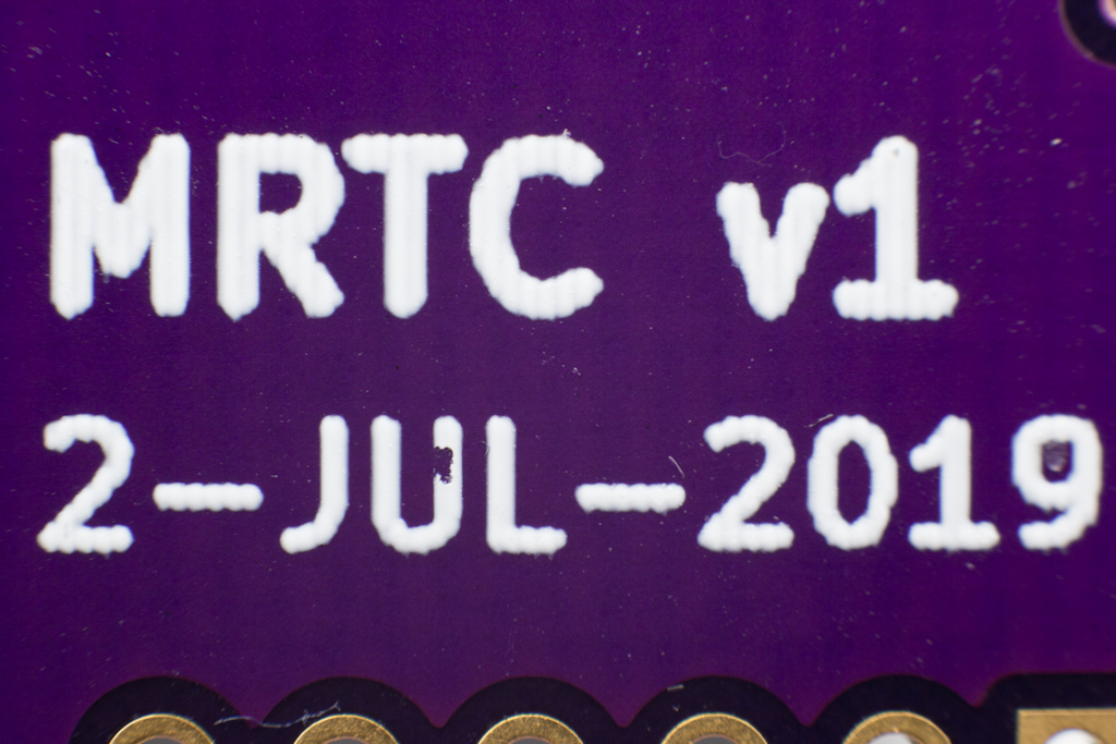
Manufacturing Reports Test Coupon v1
Lustrous Solder Mask
Thick Copper
Super Flat ENIG Surface Finish
Amazing Customer Support Response Time
Cost
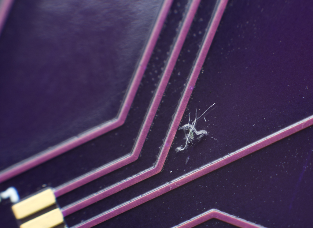
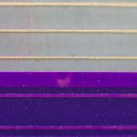
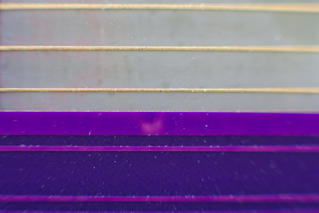
Lint Trapped in Solder Mask
Board Edges have Mouse Bites
Boards Shipped Loose In Padded Envelope
As one of the best known and most well regarded PCB prototyping services in the market, I’m excited to be writing this OSH Park PCB review. Acting as an order aggregator, they panelize multiple individual orders together to reduce the manufacturing cost for boards spun with their US based manufacturing partners. One of the prime selling points of using OSH Park as a fabrication partner, is the ease of use of the ordering interface. In addition to standard Gerber file uploads, PCB design files can be directly uploaded as well from EagleCAD and KiCad.
Cost
In the 2019 round of circuit board manufacturer reviews, OSH Park was the fifth most expensive of the 20 manufacturers surveyed, coming in at $116.80 for 12 copies of the Manufacturing Reports Test Coupon PCB. That comes to $9.73 per board at quantity 12 with standard free shipping.
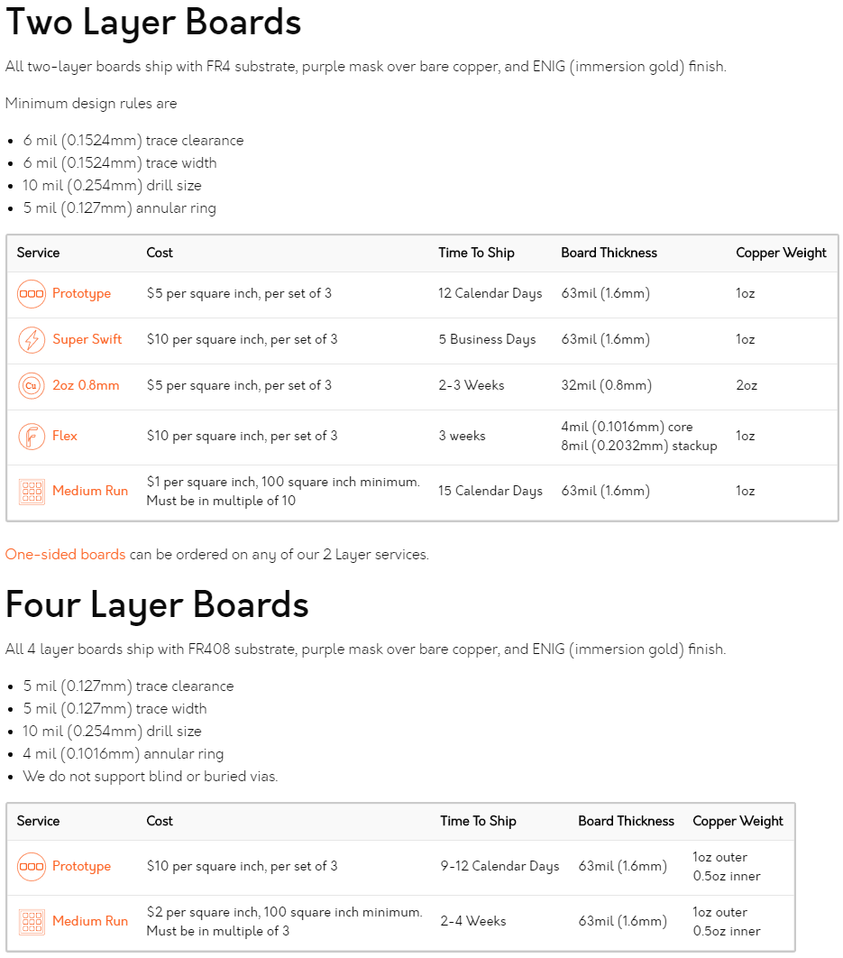
They publish a simple pricing schedule for rigid circuit boards: $5.00/sqin for 2 layer boards and $10.00/sqin for 4 layer boards (1 square inch = 645 square mm), plus applicable taxes. Those prices are for a set of 3 copies of your design and standard order quantities must be placed as a multiple of 3. Larger orders can be placed using their “Medium Run” service, at $1.00/sqin for 2 layer boards and $2.00/sqin for 4 layer boards, and require a minimum of 100sqin overall and must be ordered in multiples of 10.
Ordering
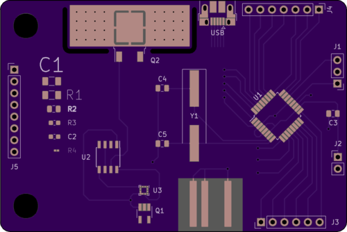
The ordering process with OSH Park was simple. Upload your KiCAD design file, EagleCAD design file, or zipped up Gerbers, give your design a name and description that will appear in your order invoice, review the board previews and pay with either a credit card or paypal. I’ve included an example of the Test Coupon v1 “Board Top” below, however every fabricated layer of your board is presented as an isolated graphic for review.
Ordering options are limited, and can only be applied to their two layer board orders. You can select 2oz copper over their standard 1oz copper service, however this does change the delivery time to 2-3 weeks rather than the standard 12 calendar days. If 1oz copper is acceptable, you can select the “Super Swift Fab” option to have your board shipped within 5 business days.
Four layer boards ship in 9-12 calendar days, but are limited to only 1oz copper on each of the layers. Super Swift Fab service is not available for 4 layer boards.
In all cases, your boards will be fabricated from a stackup of FR4, your selected copper weight, with purple soldermask and all exposed copper will receive an ENIG finish.
Delivery via US Postal Service First Class is available for free while express shipping options can be selected at checkout, if you need some form of overnight shipping.
Board designs are stored with your account on the OSH Park site, so reordering a board is very easy. Your designs can also be shared with the OSH Park community, or deleted outright at any time.
-
- Ordering Options
-
- Board Preview
Fulfillment
For this review, standard free shipping was selected for the order and I received a shipping notification seven days later, well within the 12 calendar days they promise.
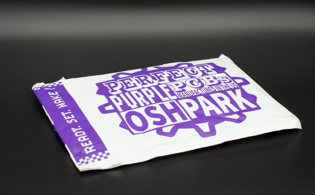
Within the entire experience of working with OSH Park, it’s the packaging that disappoints because the boards are placed loose inside a padded envelope. I much prefer having my orders vacuum sealed to keep them from banging around and sliding against each other in transit.
-

- OSH Park Order Packaging
-
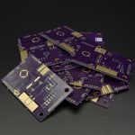
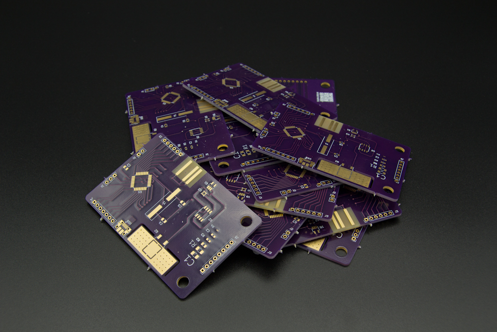
- Boards Straight From The Bag
Customer Service
Immediately after paying, an order acknowledgement is sent to the email address you submitted during the order process, however no invoice is attached. You have to go back to the OSH Park website and check your order status to download a copy of it. Status emails are sent when your board has been added to a panel, when that panel is sent to the fab, when your order has been received by OSH Park from their manufacturing partner, and finally when your order ships, although that is not reflected in updates on the order status web page associated with your account.
Design rules are clearly spelled out on the OSH Park services page. Additionally, they have extensive design tool specific support content to help customers apply the design rules correctly and cover typical mistakes that might crop up, such as not filling copper pours prior to uploading the files.
Design Tool Support
Finding the support address was easy, and a request was emailed for an order status. I had a replay within 12 minutes, and that was at 6:30PM on a Friday. I’ve worked with OSH Park before for both prototype and production work, and expected no less. No phone number or skype is published that I could find.
Their website itself is easy to navigate and figuring out how to place an order is easy. A little more information on your account page detailing the progress of an order, would be nice.
Circuit Board Visual Inspection
-
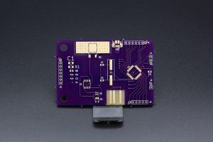
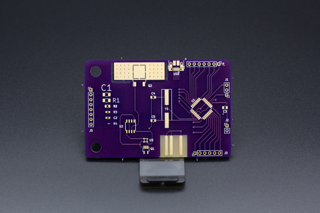
- OSH Park Full Board Front
-
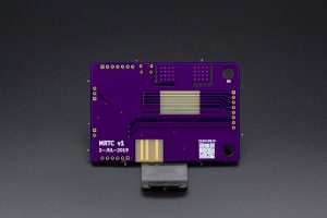
- OSH Park Full Board Back
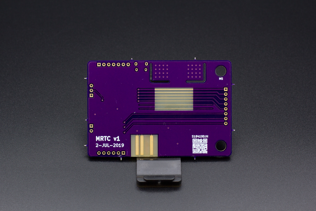
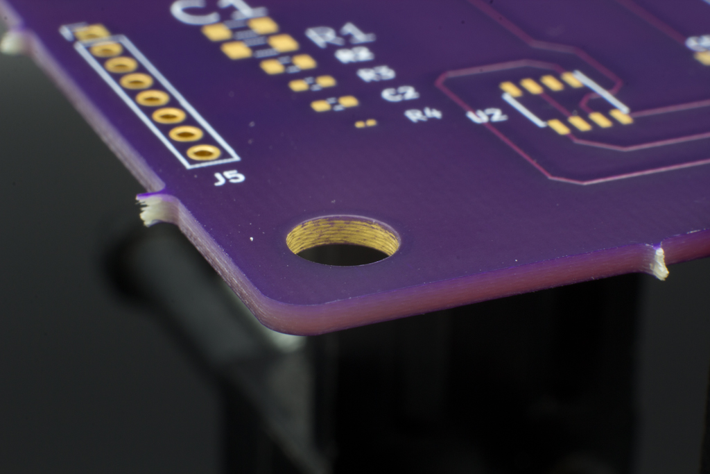
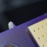
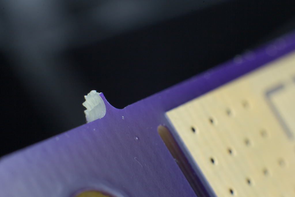
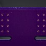
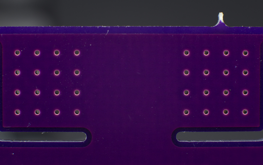
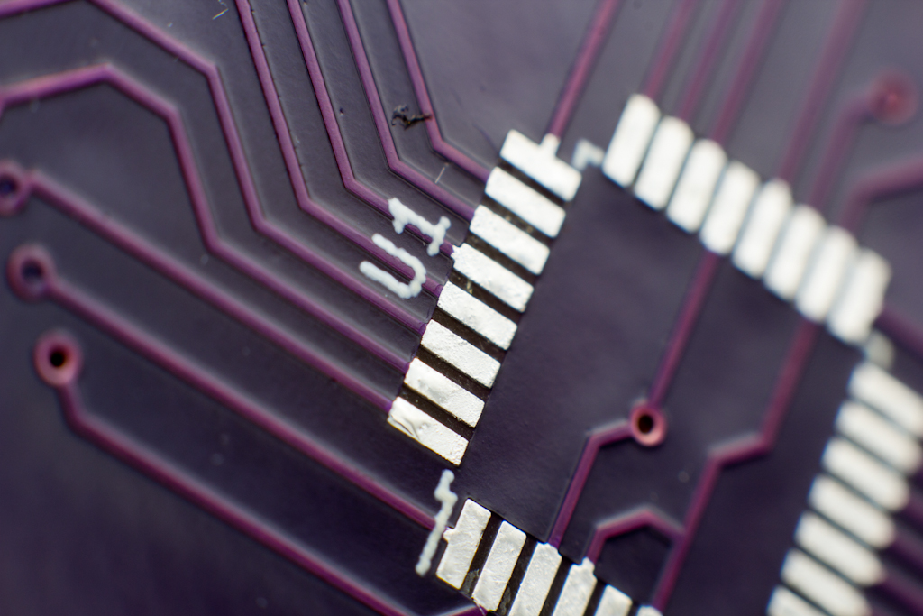
The first impression of the boards strikes you in two ways, the deep purple of the solder mask and the sharpness of the ENIG surface finish. Boards are separated at OSH Park by snapping mouse bites rather than v-groove so my fingers suffered during constant handling of the spiky fiberglass while measuring and inspecting.
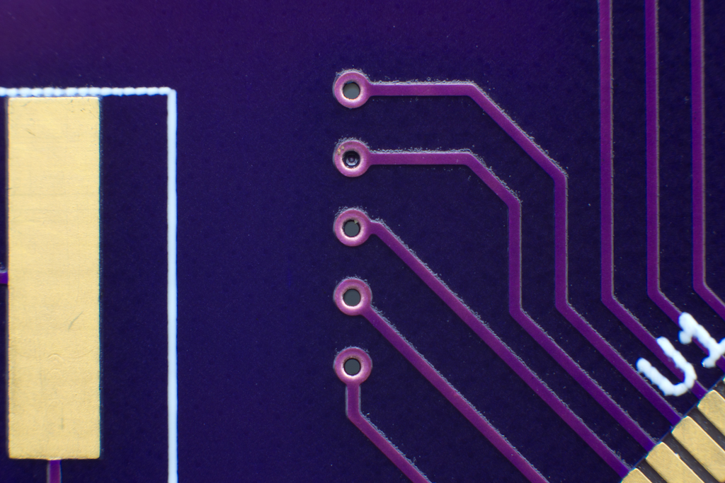
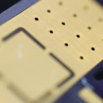
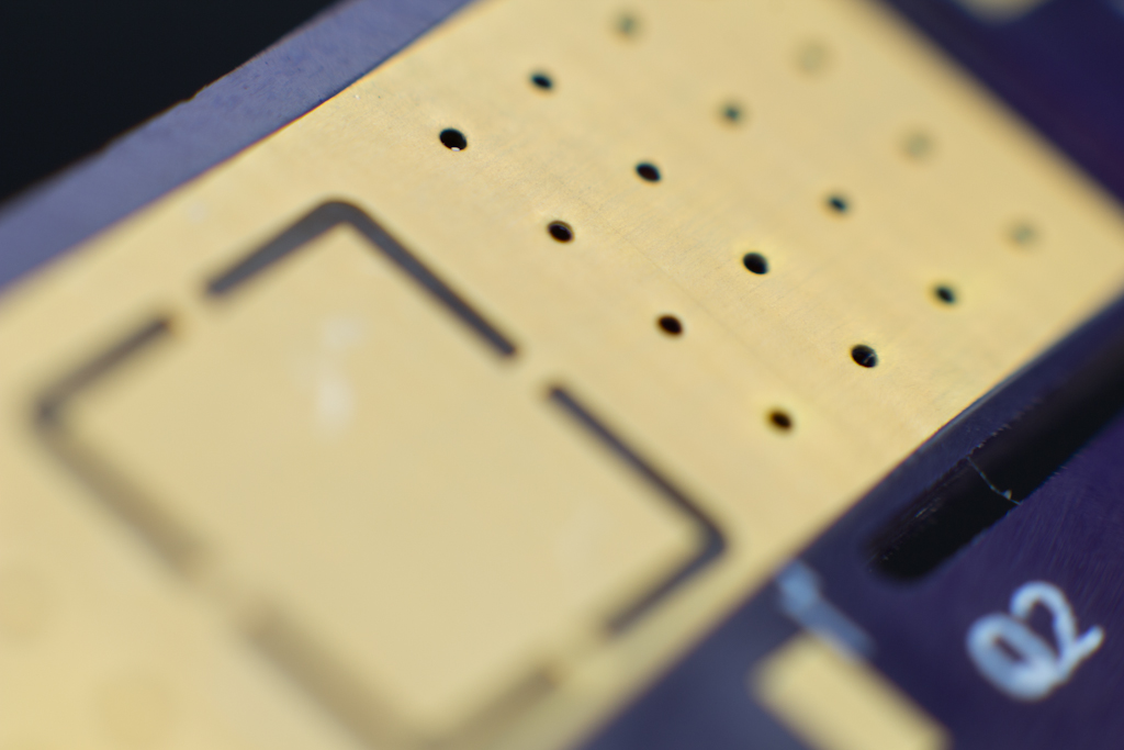
The via drills are on target with a few exceptions on one board that were slightly off center, and the milled slot was fabricated correctly. For some reason, the mechanical holes were plated, but testing with a DMM showed that the conductivity was isolated and disconnected from any traces or copper pours.
Boards 04, 05 and 10 didn’t receive a single negative mark at all outside of having low resolution direct legend silk printing. They were some of the highest quality boards I’ve evaluated.
PCB Dimensions
All dimensions measured to within tolerance. Board edges were all slightly over sized by 0.1mm while the mechanical holes were all slightly undersized, but only at most by 0.05mm, and had no issue mating with the test jig. The internal slot around the heat sink was within 0.01mm of the dimensions specified in the design files.
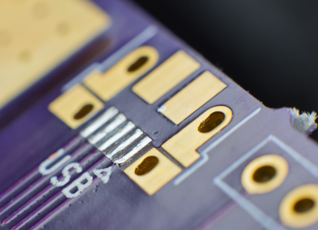
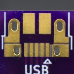
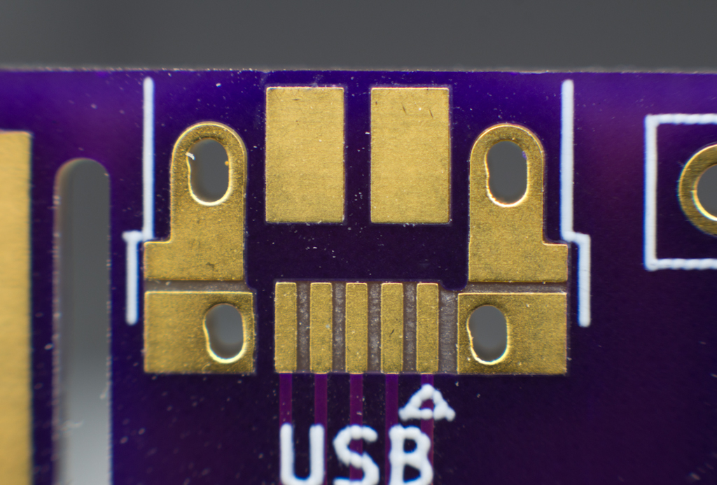
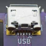
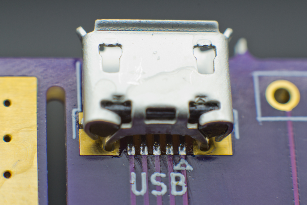
Trace widths were either directly to spec or measured 1 mil under, within tolerance even for the 6 mil trace, and plated slots for the USB footprint is my only quibble with footprint reproduction as quite a few boards showed slots that were more potato-shaped than directly perpendicular to the board edge.
-

- OSH Park Via Drills
-
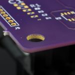
- Plated Mechanical
-
- Offset Plated Slots
-
- Mouse Bite
Copper Layer Quality
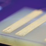
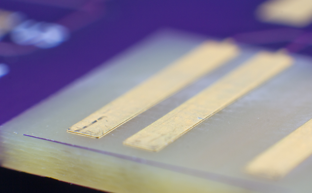
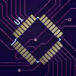
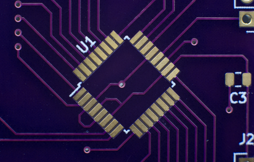
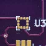
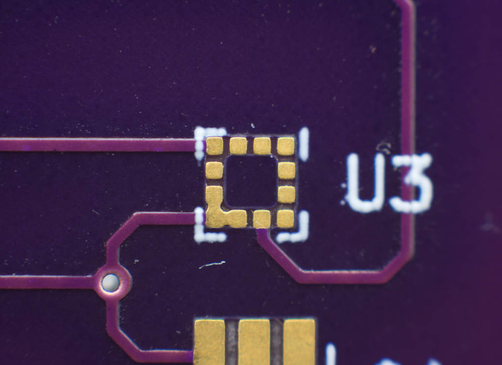
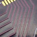
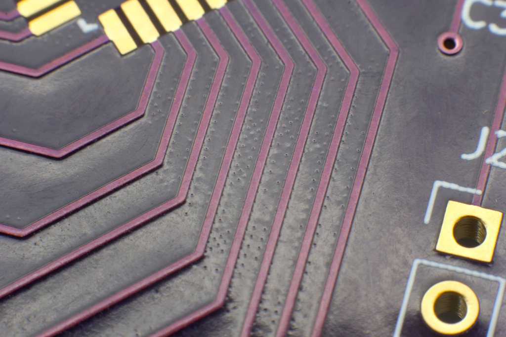
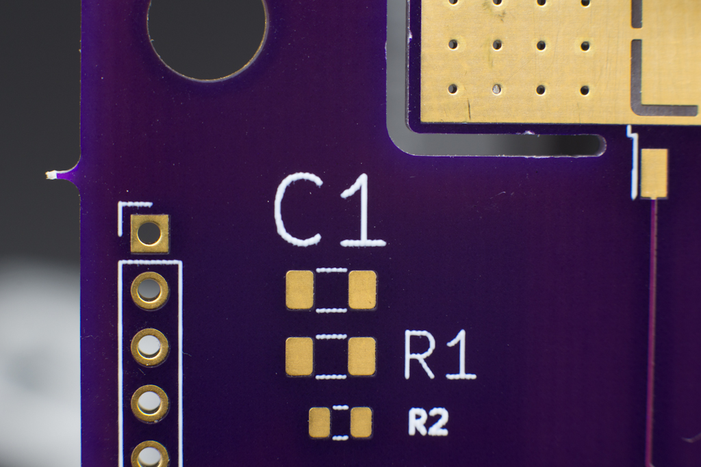
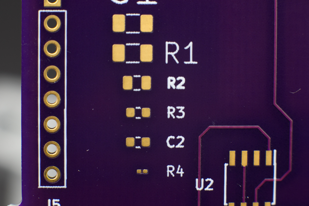
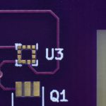
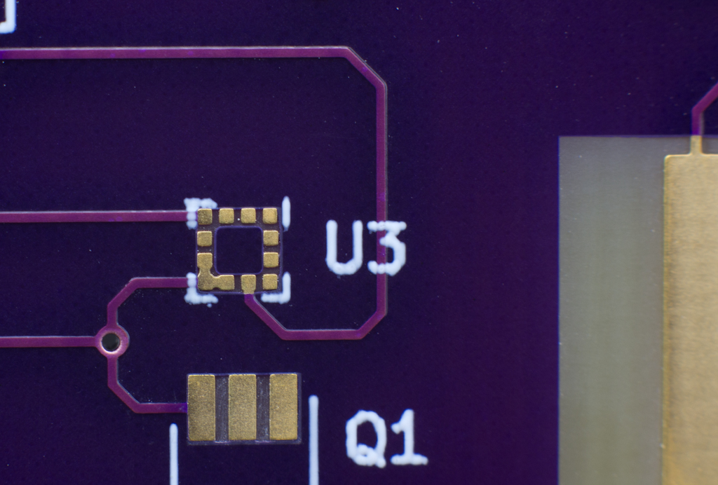
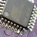
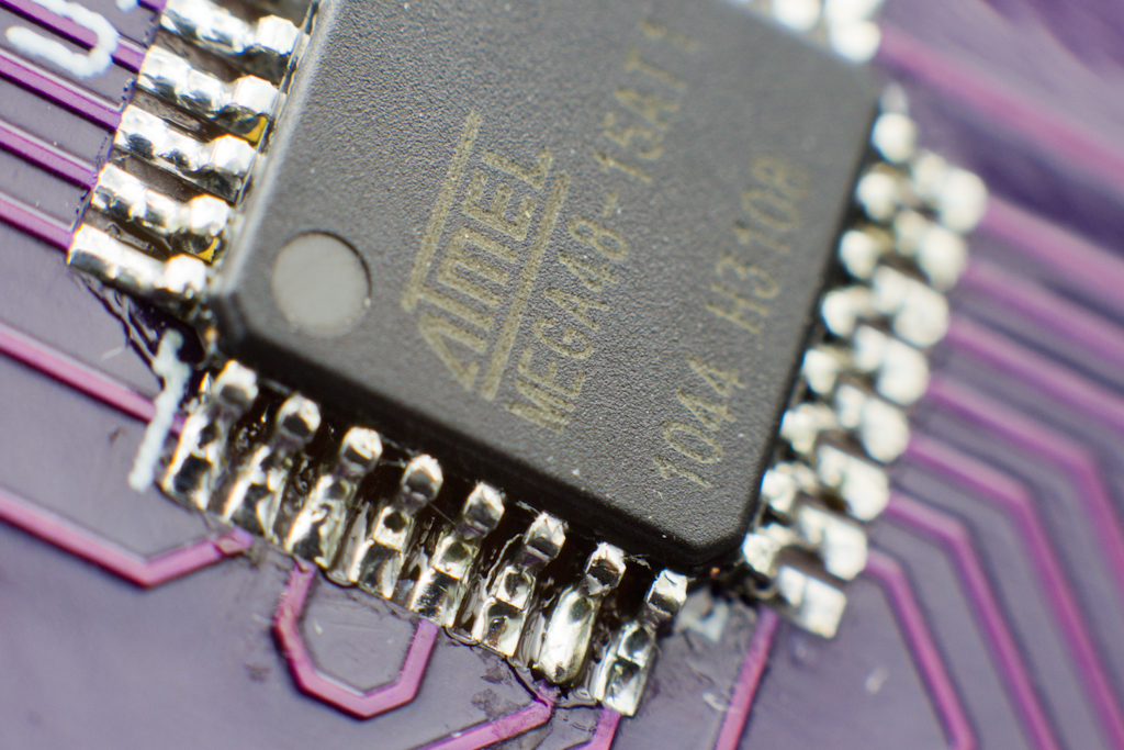
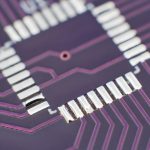
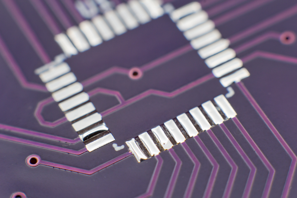
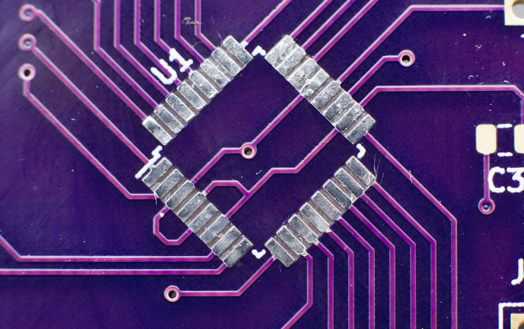
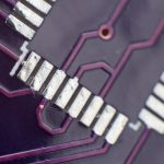
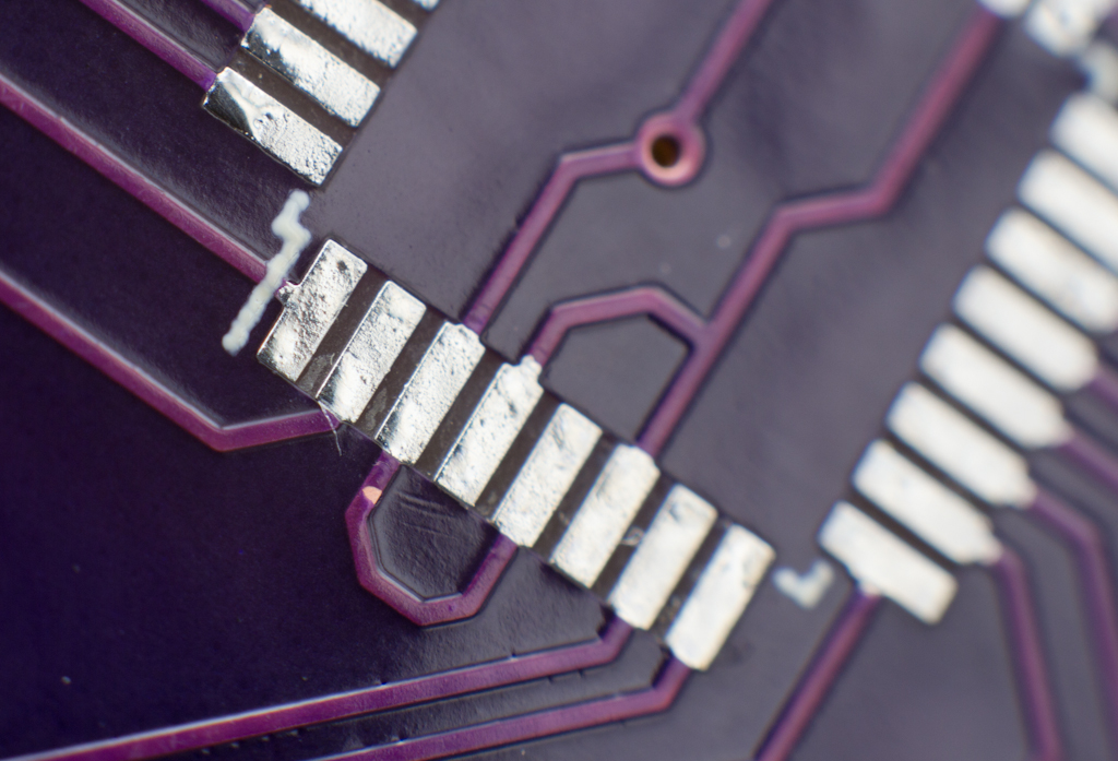
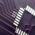
The copper quality of the OSH Park boards is absolutely stellar with an ENIG finish universally applied. That surface finish really shows off the minuscule pads of the QFN footprint well. Copper weight measured above the expected 1oz, with the thinnest test pad measuring right on spec at 1.4 mil, the thickest 4.0 mil and the average being 2.7 mil.
All passive footprints were reproduced correctly from the 1206 to the 0201 and all had a thorough ENIG deposition. The QFN and QFP footprints look stellar, clean and very planar, and while OSH Park doesn’t get an extra score for the ENIG, as it’s the only option, you certainly do get what you pay for.
-
- Pad Thickness
-
- QFP Footprint
-
- QFN Footprint
-
- Copper Pour with ENIG
Solder Mask Quality
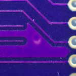
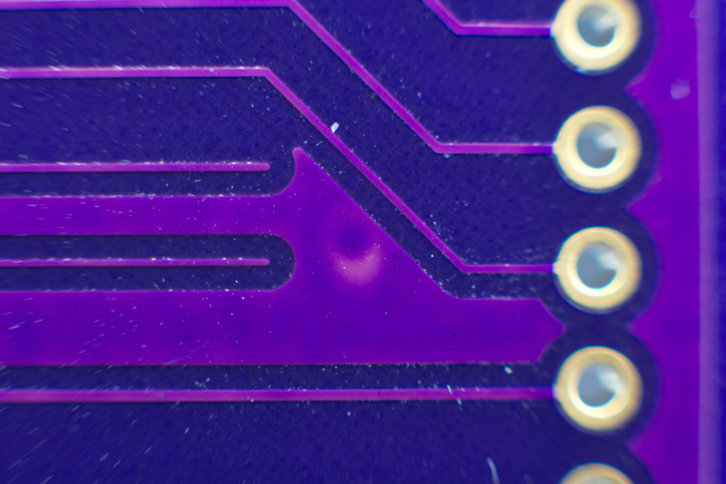
The solder mask quality is where I saw some flaws. There was contamination on the surface of several boards and strange patterns appeared to have been impressed into others during fabrication. On the back side of three boards there were strange halos that didn’t seem to be associated with substrate delamination at a drill site, so it left me a bit confused.
Board 02 had something that looked almost like small drops of dried liquid in the center of the board that couldn’t be scraped off or washed clean with 99% Isopropynol. Board 06 had some fuzzy blob of something baked into the solder mask right next to the trace.
Boards 01, 03 and 07 all had strange halo like markings in the mask layer, of an origin I couldn’t determine without performing a destructive test. As mentioned above these didn’t appear near drill positions so I don’t believe them to be associated with some FR-4 issue, so they wouldn’t appear to affect the functionality of the board however the mask quality score did suffer due to the lack of uniformity.
Boards 06 and 09 also had the solder mask butting up against the pads, and had the pad thickness been any smaller, I believe the mask would have covered the pad edge.
On the positive side, the solder mask applied over the heat sink area is spectacular. It is exceptionally well executed with a nice thick and consistent layer of mask over the via stitching, and no sign of significant wicking or sinking to speak of.
-
- OSH Park Gorgeous Solder Mask
-
- Lint Bonded To Solder Mask
-
- Surface Contamination
-
- Strange Pattern in Solder Mask
-
- Solder Mask Halo 03
-
- Solder Mask Halo 02
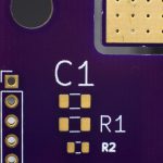
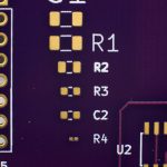
Silkscreen Quality
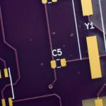
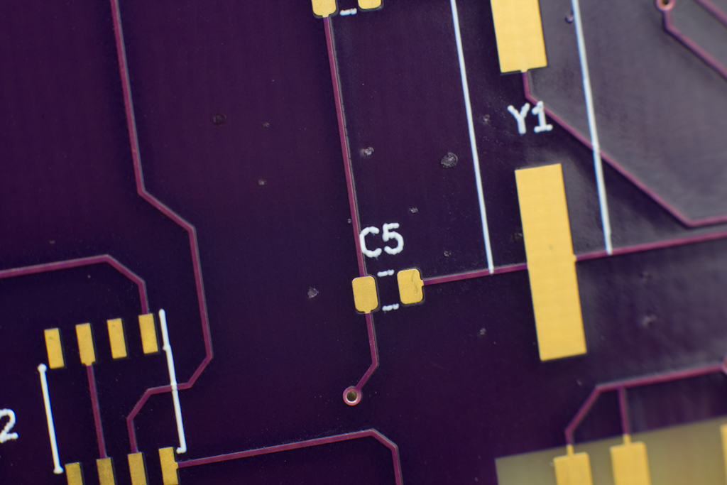
Silk screen is applied through the expected low cost direct print method, and it seems to be printed at fairly low resolution. It is evenly applied across the surface with no change in quality when printed on varying z-depths as may occur over traces. All the reference designators are legible, including the test print area by the passive footprints. There is only one single misprint and it is exceptionally minor, the “U” in “JULY” on one board has a small nick in it.
-
- Silkscreen Passives Area 01
-
- Silkscreen Passives Area 02
-
- Silkscreen Print Over Trace
-
- Damaged Character
-
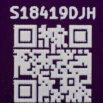
- QR Code Resolution
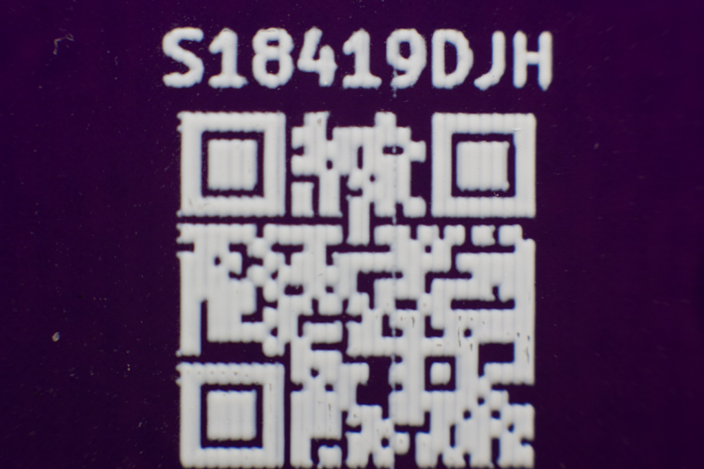
The 1cm QR code would not resolve, even with magnification.
Solderability
The Micro USB and QFP32 components were soldered onto their footprints, and the ENIG plating makes it very easy to align the pins as the color contrast between pin and pad makes for easy viewing. The uniform surface of the pads also allows the component to sit solidly on the footprint while soldering.
The QFP32 footprint was robust throughout the rework process, showing very little erosion to the solder mask and no damage at all to the pads. I had problems with the flux in the solder wick, and had to apply it multiple times after the first rework to clean the pads, however that didn’t seem to have any noticeable effect. The only erosion I found was on a single trace on the southwest portion of the footprint.
When working with the Micro USB Connector, it soldered easily and showed very small amounts of solder mask erosion after two rework cycles, demonstrating some of the best mask durability I’ve seen.
After the rework, the silk screen looked completely unscathed from the repeated heating, washing and drying.
-
- QFP32 Initial Soldering
-
- Micro USB Initial Soldering
-
- QFP32 After First Rework
-

- QFP32 After 2nd Rework
-
- Rework Mask Erosion
-
- Rework Silkscreen Undamaged
-
- Micro USB After Rework