Seeed Studio PCB Service Review
Seeed Studio
Shenzhen, China
$0.49
5-6 Days
Manufacturing Reports Test Coupon v2
Incredibly Cheap Cost
Excellent HASL finish
High quality fulfillment and order packaging
Mostly matched or exceeded 1oz copper thickness
Limited Stackup Options for Prototype Service
Added to marketing email list by default
Thin solder mask
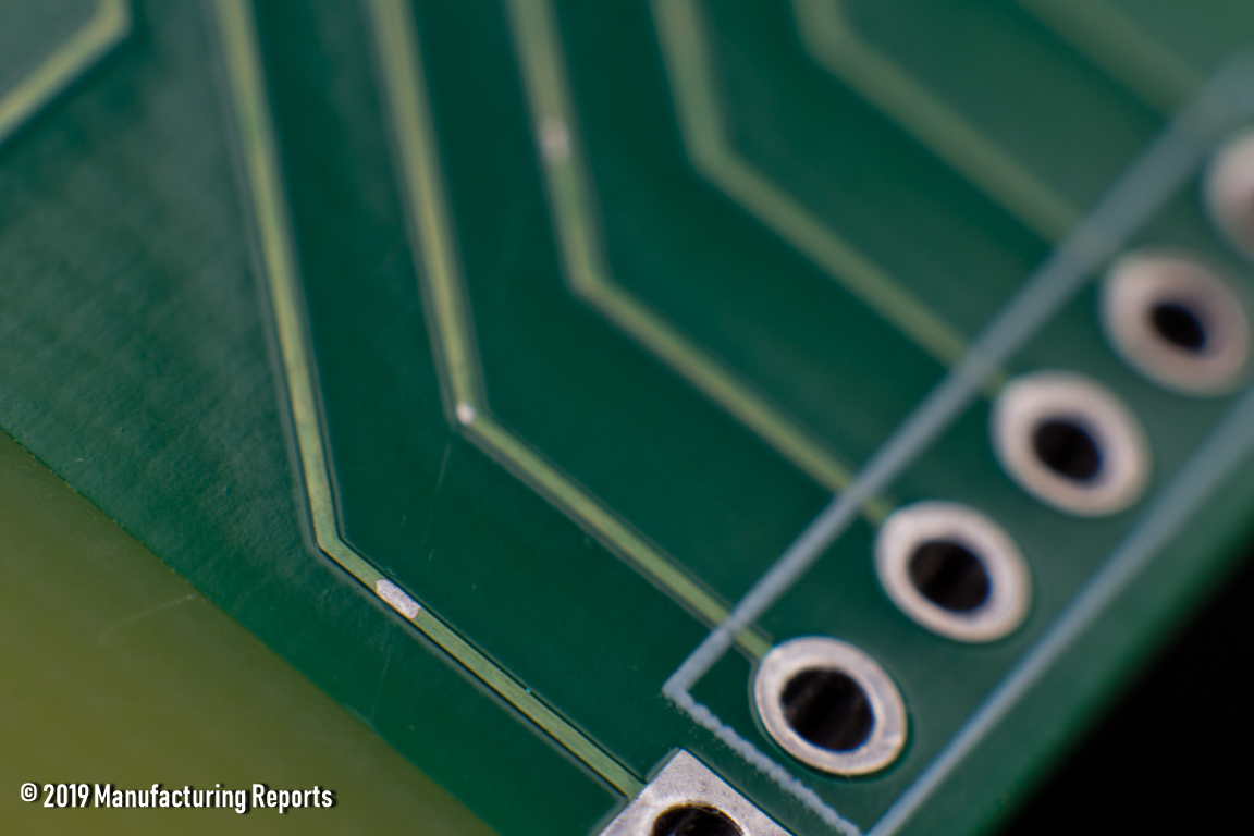
Many traces exposed by scratches
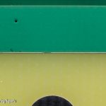
Very high limit on solder mask web width (12 mil / .32mm)
Seeed Studio used to be known primarily as a retailer of Arduino clones, Raspberry Pi accessories and their line of “Grove” interconnecting breakout boards. They’ve grown out a circuit board fab, electronics assembly service, 3D printing service bureau and CNC Machining capability, and this Seeed Studio PCB Service Review will focus on their Fusion brand, targeted squarely at “global creative technologists”, independent engineers and tinkerers. While their headquarters are based in Shenzhen, they opened an office in San Francisco in 2015 and in 2017, opened offices in Nagoya, so they would seem to be trying to push the Seeed brand regionally through local offices more than any other low cost EMS or fab.
Cost
Seeed is charging $4.90 for 10 copies of the Test Coupon, which comes in just under the $5.00 order cost from JLCPCB and PCBWay. This is no surprise as cost of PCB fabrication has become a run to the bottom offshore. Of course, Seeed also charged me $20.72 for DHL shipping. The exact same order, for the exact same board, using the exact same shipper, getting delivered from the exact same city in China, costs about $4.00 more through Seeed. Shipping costs are a nebulous realm of individual contracts between manufacturers and logistics companies based on volume and who played golf with who recently, so it may be that JLCPCB gets better rates than Seeed, or it may be that some manufacturers are padding out non-existent margins on loss leader services by squeezing a few extra dollars out of shipping costs.
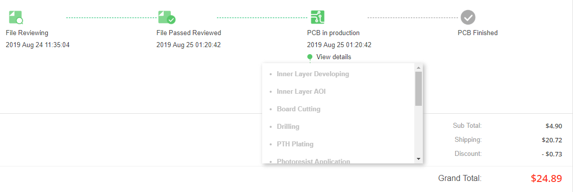
Anyway, total cost for the order was $24.89 after a random $0.73 discount was applied.
Ordering
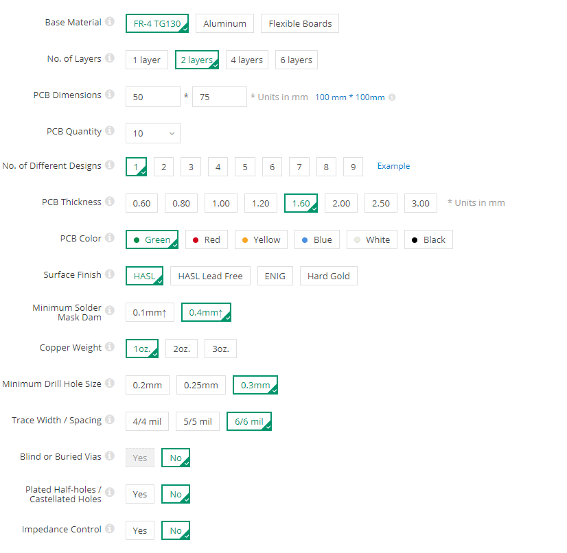
Prototype ordering options and stackup are selected through the typical interface, and defaults were selected. The subset of prototype service options is on the more limited side, with what seems like a focus on providing services to those who want to make blinky badges and circuits of that nature. One unique option I saw on Seeed’s site was the possibility of a Hard Gold surface finish, that increased the price from the promotional $4.90 for 10 units to $216.92 for 10, and doubled the production time from 3-4 days to 6-7.
Gerbers were uploaded and after clicking on the shopping cart icon to checkout, you are presented with a screen to create an account first. After doing so, all the order options and gerber upload was wiped out and had to be recreated. Then after adding that to the shopping cart, both board batches magically appeared and the second one had to be deleted.
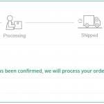
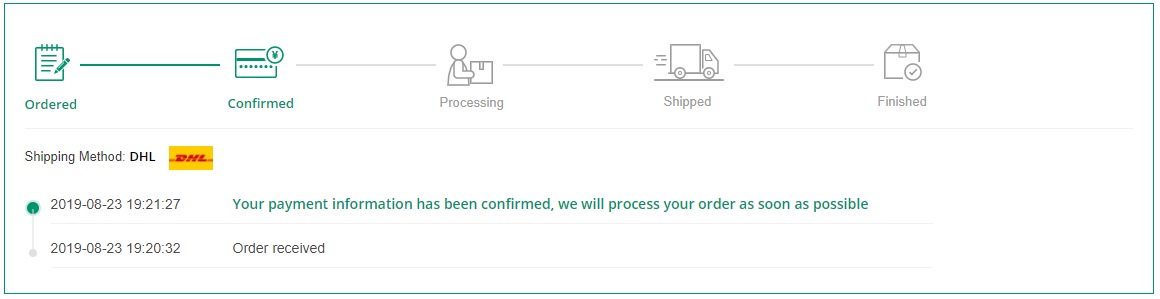
Payment is handled with Paypal, and I was quoted 3-4 days production time with 1-2 days delivery after shipping. Immediately after the payment went through, the order appeared in the Account Management page on Seeed’s site, showing the options selected, and a link to a well formatted invoice. A cute if rudimentary order status graphic is provided in the order detail screen, but it’s not of much use.
No gerber preview or board renders are provided during the checkout process, and no option was presented to eliminate a manufacturer’s mark.
-
- Seeed Ordering Options
-
- Order Status
Fulfillment
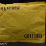
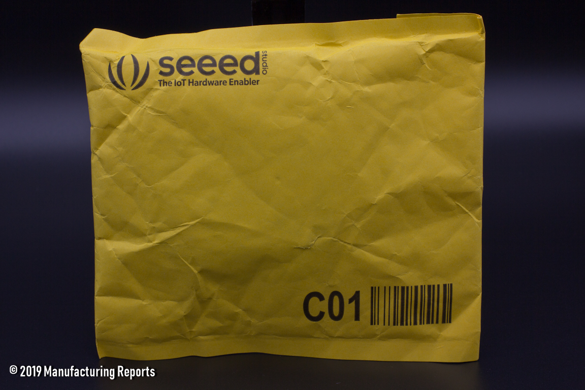
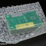
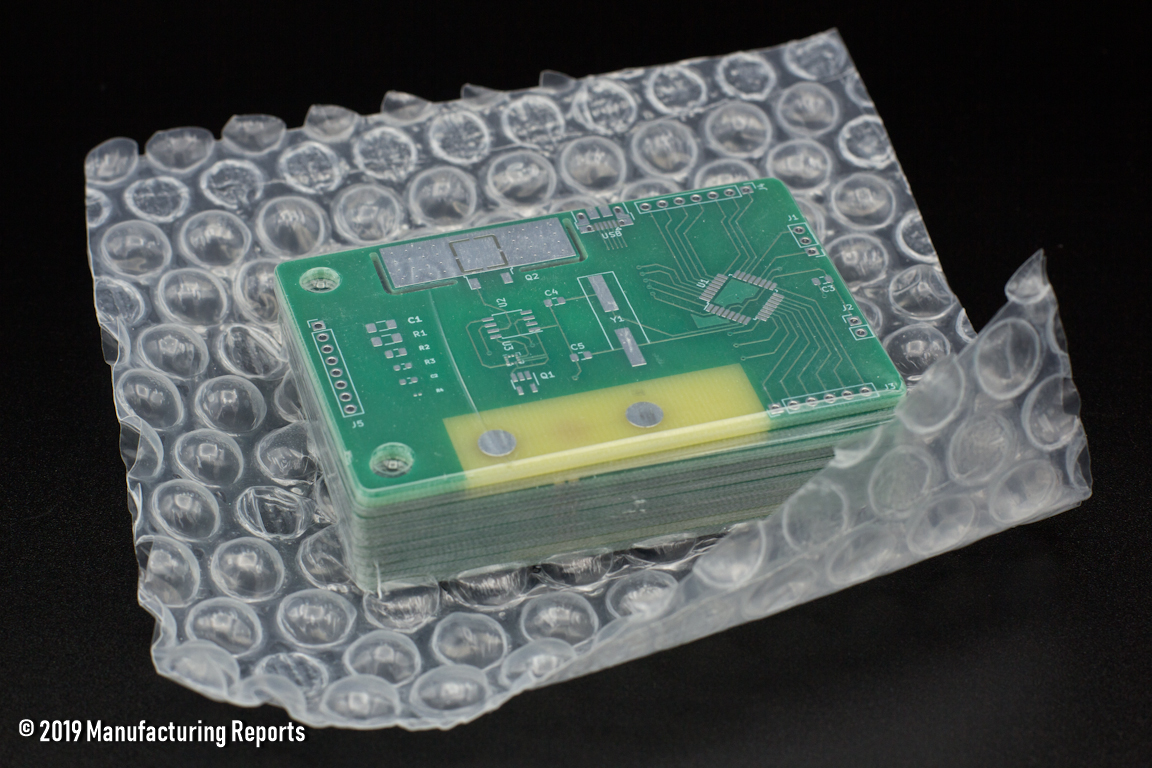
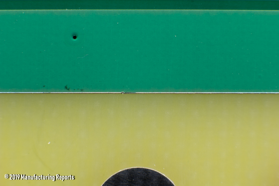
The expected ship time was four days and I received the tracking number in 3, so full marks to Seeed for exceeding my expectations on the shipping front. The boards arrived in the standard DHL vinyl envelope, and inside was a Seeed branded padded envelope and inside of that was the standard vacuum sealed bubble pouch. Definitely secured from damage.
-
- Bubble Envelope
-
- Vacuum Bubble Packaging
Customer Service
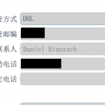
Finding who to send a customer support email to for a board order was tricky. On the Contact Us page, they had a list of six different email addresses of which three might be correct: Fusion Service, Manufacturing Service or Tech Support. I selected the Manufacturing Service email address and sent a message asking them to verify the ship to address. I received a response a few days later with a screen capture of their internal order entry system showing a correct address. I made logical assumptions as to what the Chinese characters meant.
Checking on the status of the order at first doesn’t show much, other than “Your order was confirmed and we’ll start working on it as soon as possible.” which didn’t change after several days. Looking a little further down the order status page I found a production status detail window, which would seem to show a time stamp for various manufacturing stages, but at the time hadn’t been updated yet.
Their Design Rules are easy to find by googling, at least as far as “Seeed Studios” goes. However since they have several different service options, it can be difficult to decipher which set of rules you’re looking at. For example, on the “solder mask dam” page it lists an acceptable width of 4mil / 0.1mm, however on the Fusion PCB specification page it says 12mil / 0.32mm.
Frustratingly, submitting an order to Seeed added me to their marketing mailing list, which I don’t recall having an explicit Opt-In for.
-
- Ship-To Address Review
-
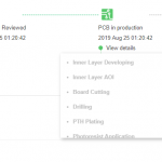
- Manufacturing Status
Circuit Board Visual Inspection
-
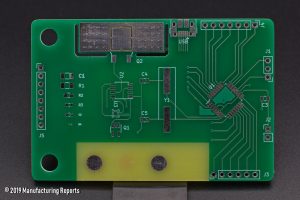
- Seeed Studio Review Full Board Front

-

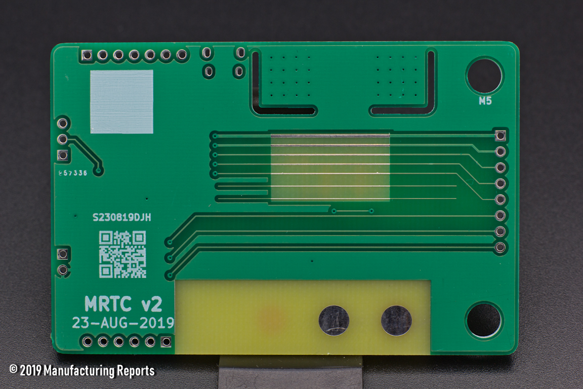
- Seeed Studio Review Full Board Back
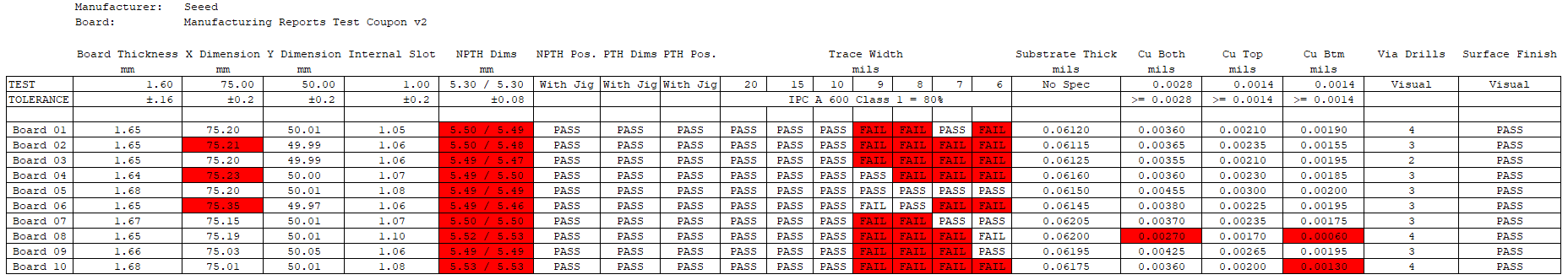
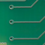
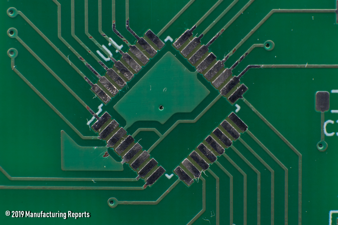
Let’s start on the positive side: the HASL was uniformly consistent and super flat across all 10 boards. Beyond that, there is much opportunity lost on these boards. When I first opened the packaging, I thought they looked magnificent, but that quickly became disillusionment as I saw how thin the solder mask layer was. Detailed inspection discovered a lot of abrasion problems and significant post-manufacturing scrapes and scratches.
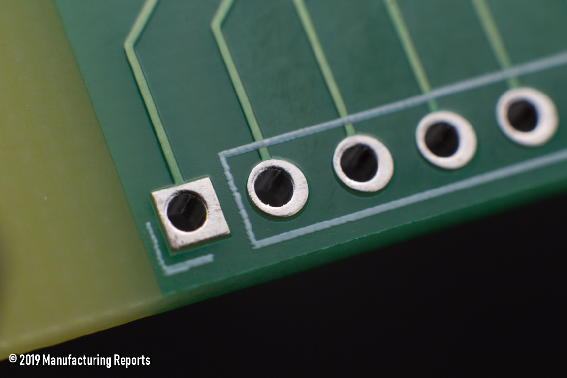
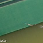
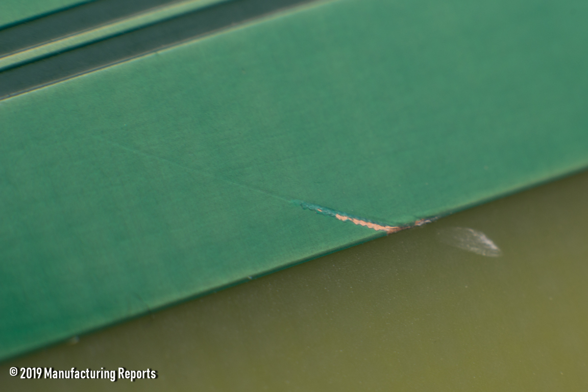
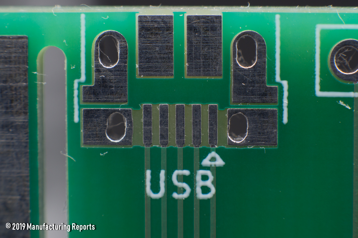
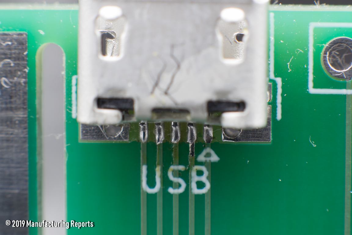
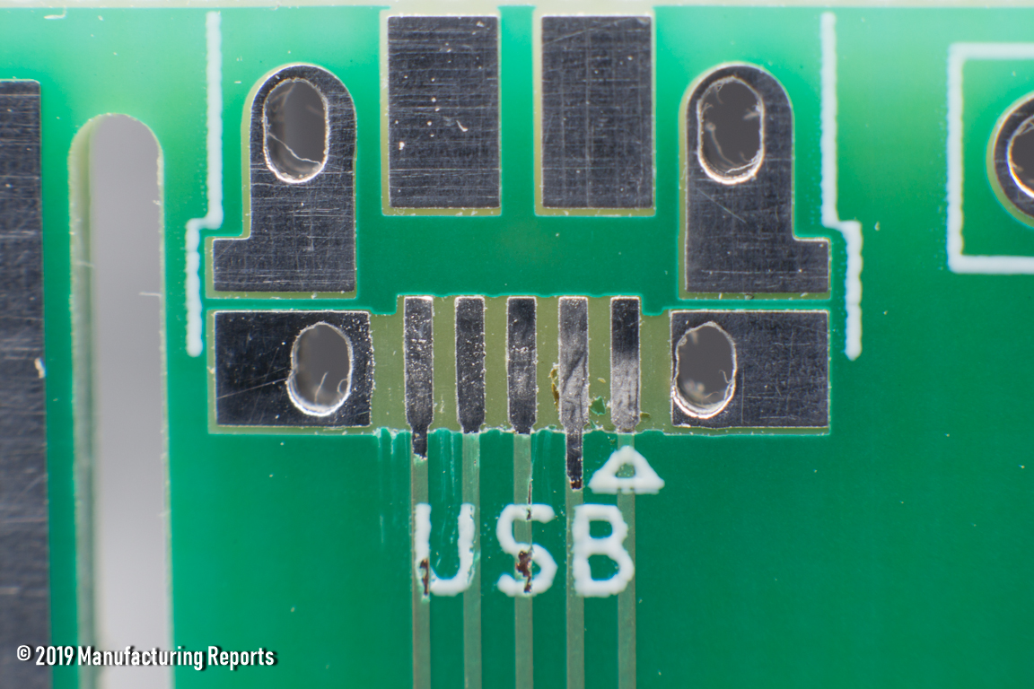
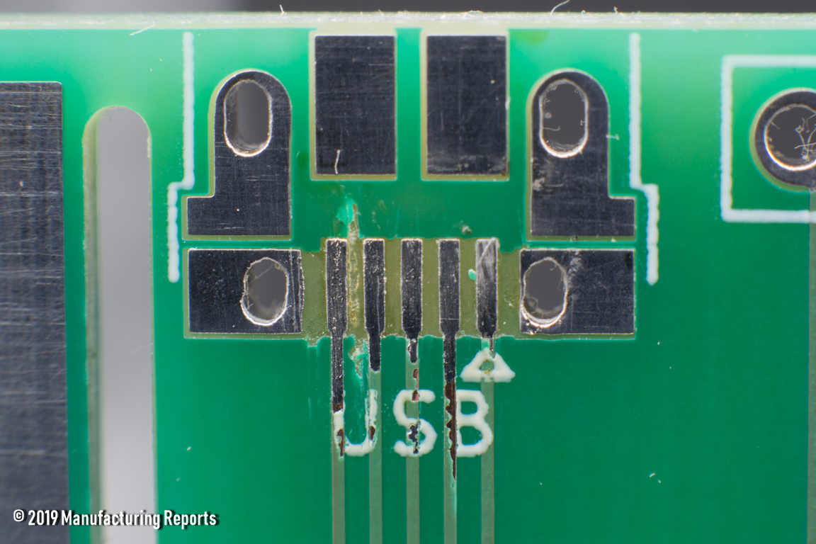
The M5 Clearance drills were all oversized and out of tolerance on all boards, and a very pronounced witness mark on the board outline forced the X-dimension out of tolerance for most as well. The via drills were all slightly or very offset, and in some cases the plated slot for the USB was fabricated nearly out of the pad.
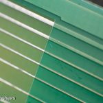
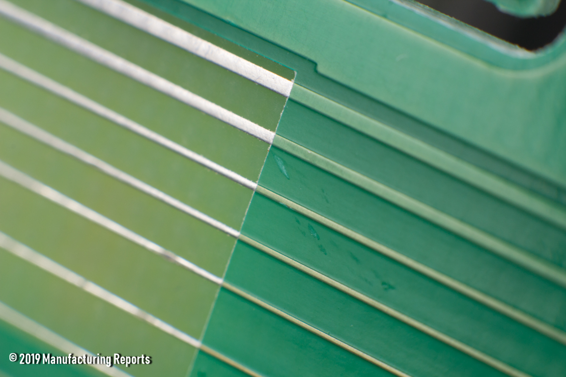
Trace widths were uniformly undersized, dramatically so in some cases. The copper thickness equaled or exceeded 1oz weight with the exception of a single board having a back side copper thickness less below 1/2oz.
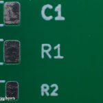
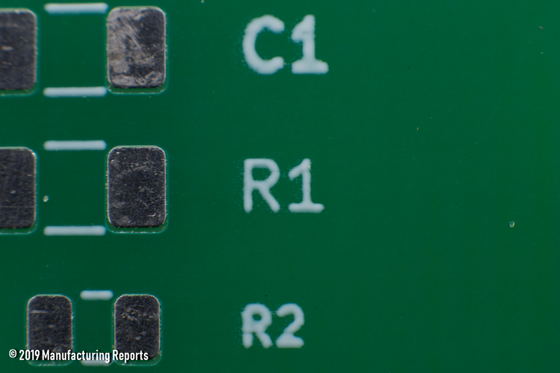
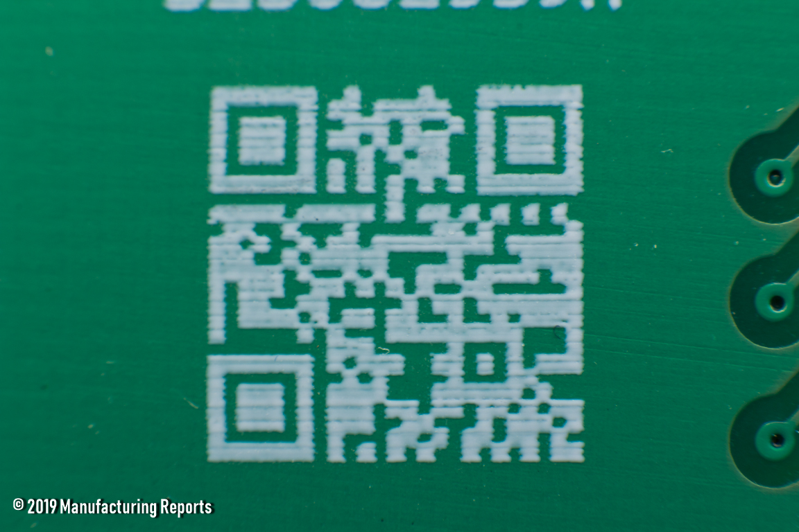
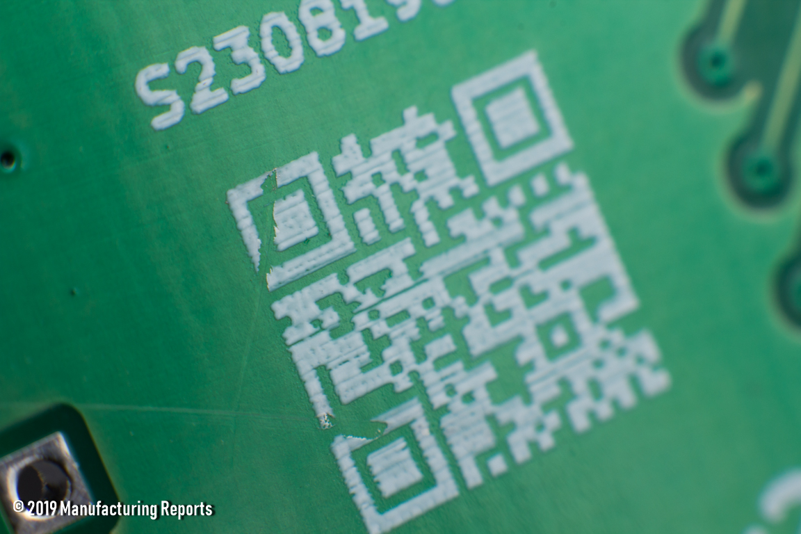
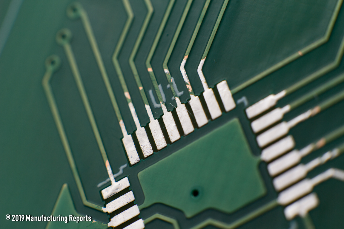
The quality of the silk screen was what one would expect from the Direct Legend Printing process, but the quality of the smallest fonts was as surprisingly good as the resolution of the QR Code was surprisingly inconsistent.
PCB Dimensions
It’s infrequent that there is a problem with the milled features of boards, however all the Seeed Studios PCBs reviewed were outside of tolerance for the M5 clearance holes, and the outer edges of many had a witness mark that stuck out beyond the +/- 0.2mm tolerance. I should note that I couldn’t find a milled feature tolerance on Seeed’s website beyond those that appear on their Seeed Studio Fusion Design Rules page which lists milled non-plated slots as +/- 0.15mm.
Speaking on non-plated slots, they were milled well within tolerance.
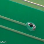
The PTH and NPTH features were correctly spaced when tested with the positioning jigs here at the lab, but because of the size of the mechanical holes, the fit was quite sloppy. The PTHs did seem offset slightly to the left in the X dimension, but not dramatically so. Enough that it was visible with the naked eye however.
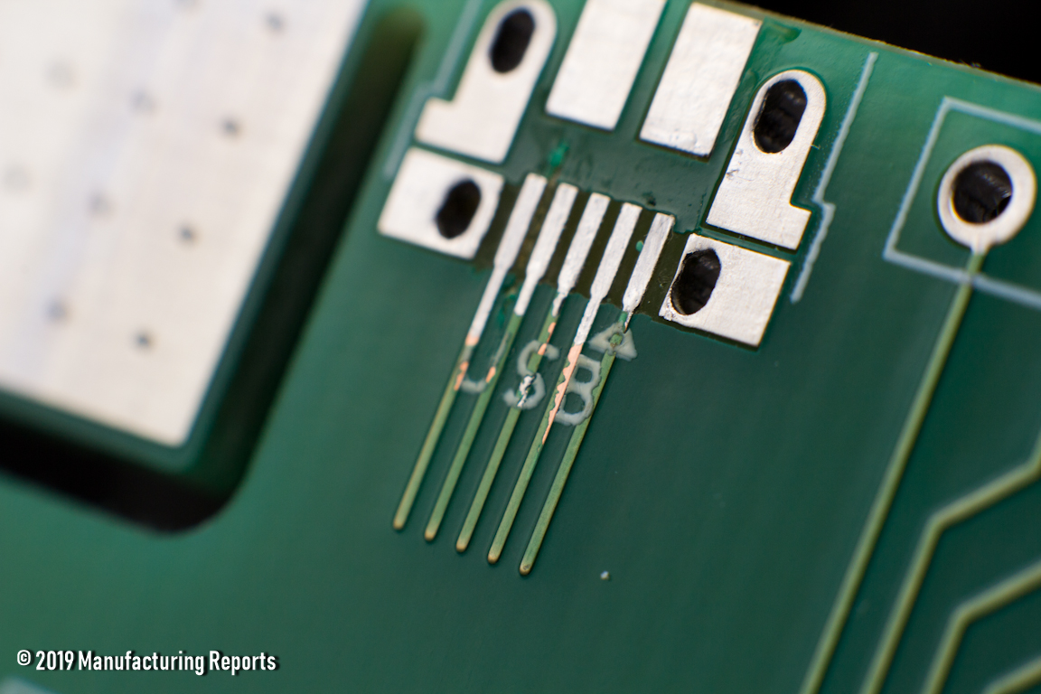
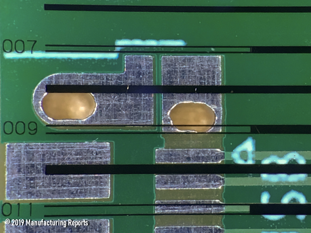
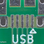
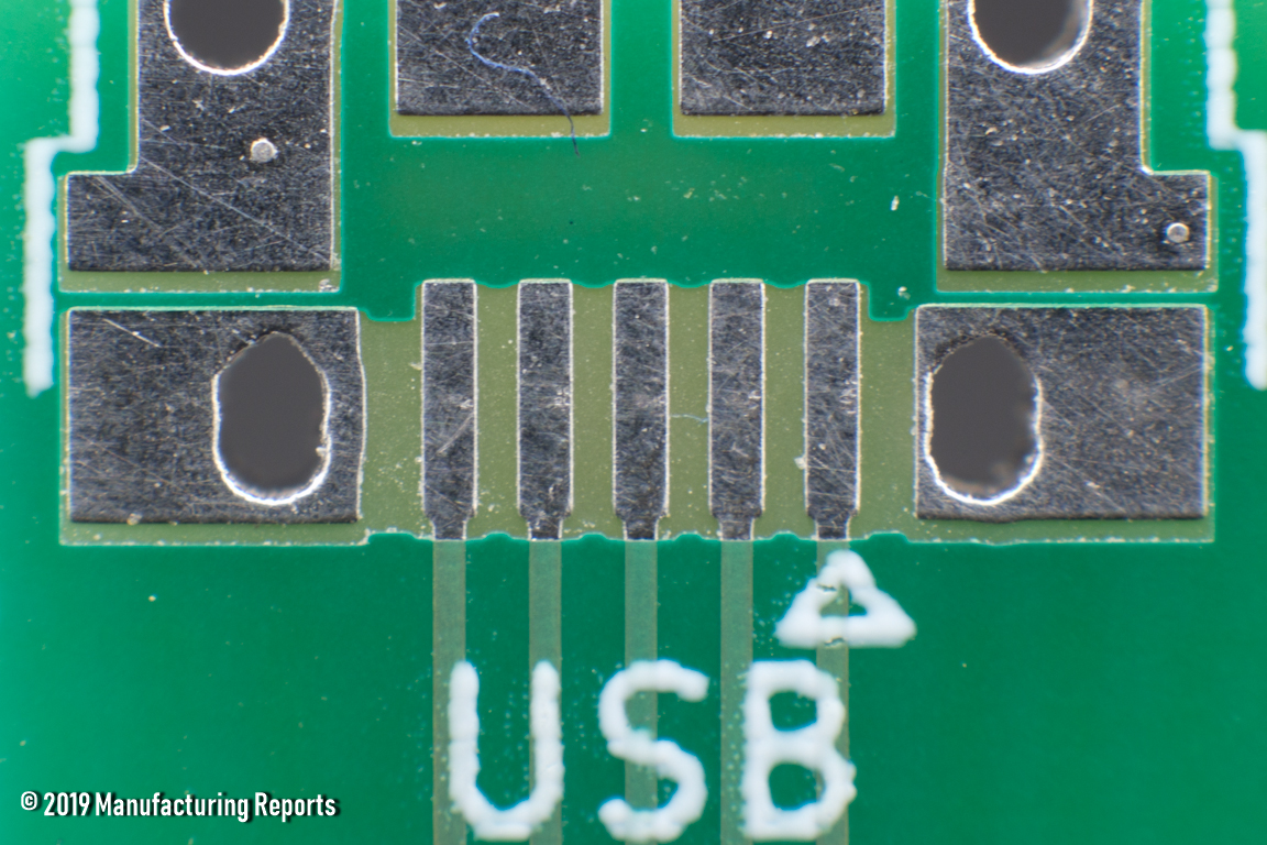
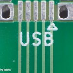
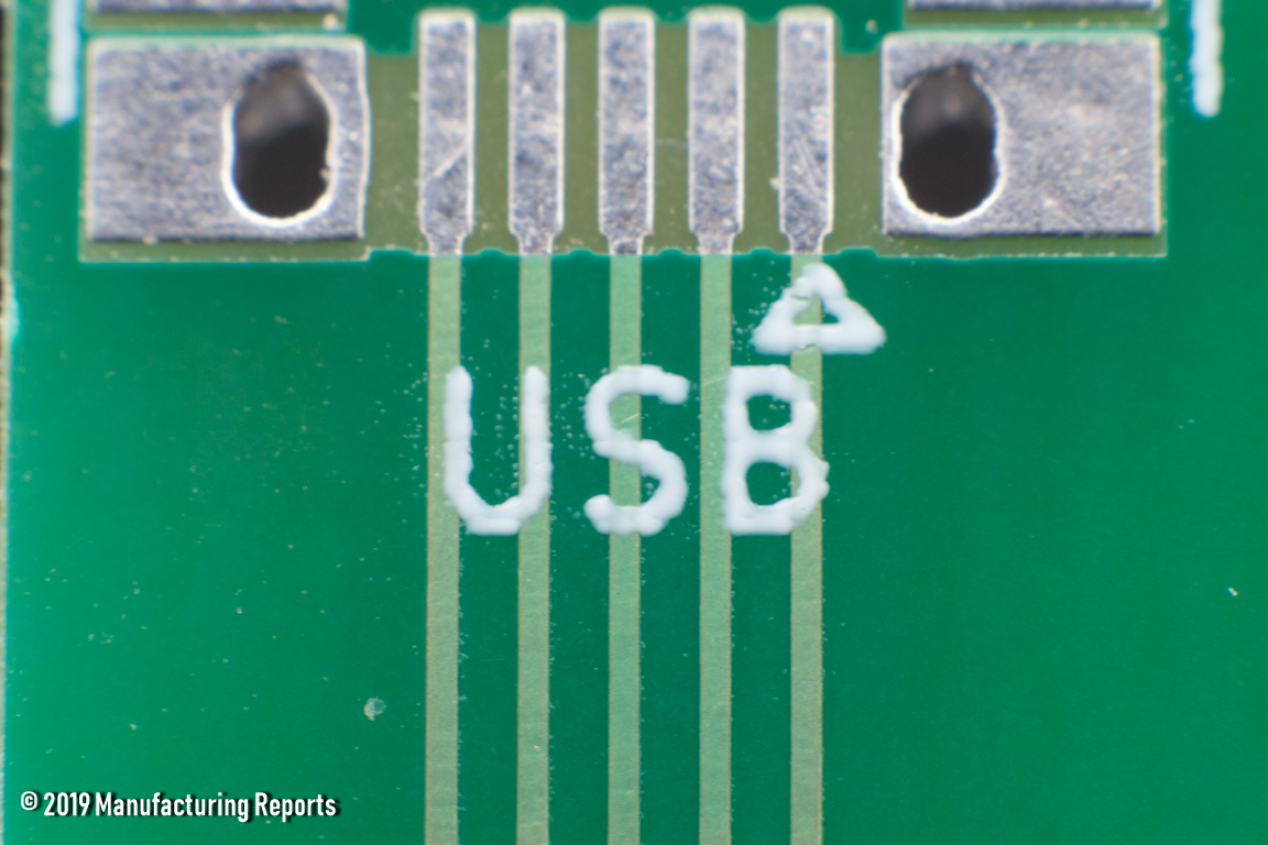
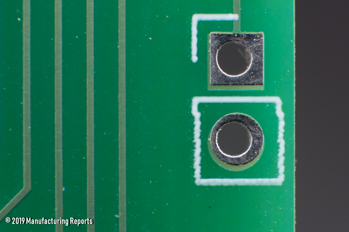
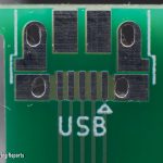
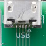
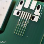
The USB plated slots were very straight, however the placement of those slots was suspect, coming very close to the edge of the pad in many cases.
The trace widths were within tolerance down to 10mil, but below that, things quickly got out of hand, measuring between 2 and 3 mil narrower in many cases. As mentioned in several other reviews, trace width is critical in determining how much current that net can carry, so if you need to use Seeed, oversize your traces considerably.
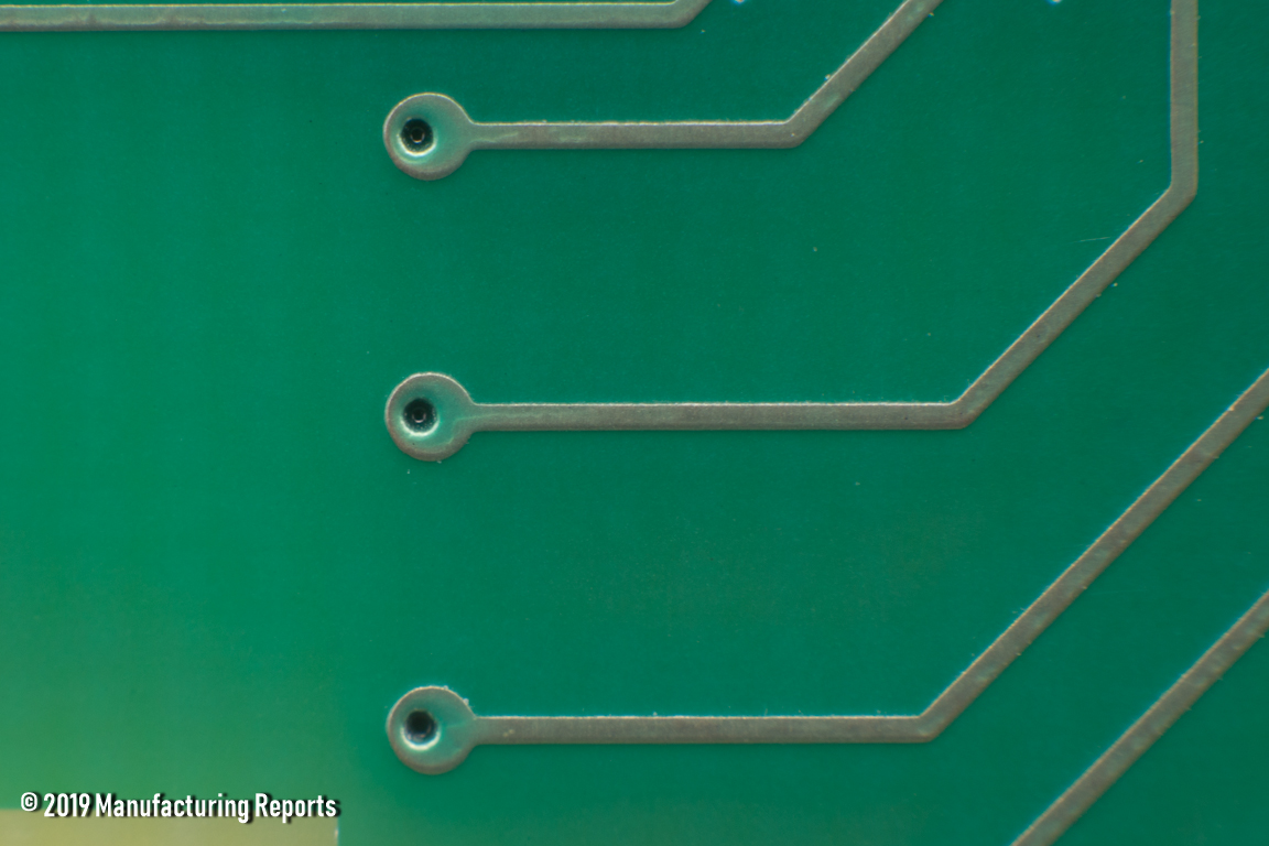
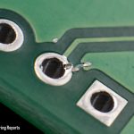
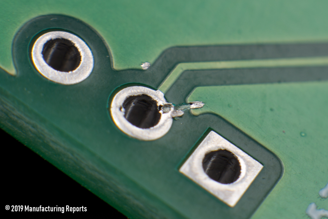
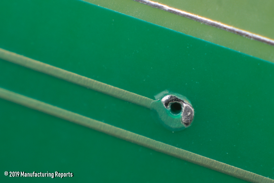
Vias were offset on all boards. In one case, the only reason the drill didn’t nick the edge of the annular ring, arose from the drill getting mashed so hard into the copper that it deformed the pad out of round.
Seeed Studio Test Report 2019
-
- Plated Slot Offset To Pad Edge
-
- Edge Cut Witness Mark
-
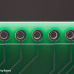
- Offset PTH Drills Top Edge
-
- Offset Via Drills
-
- Slightly Deformed Annular Rings
-
- Offset PTH Drills Btm Edge
Copper Layer Quality
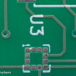
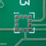
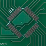
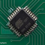
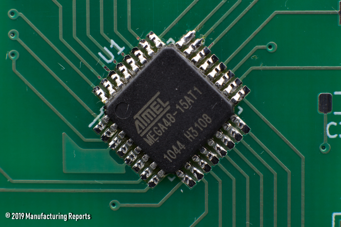
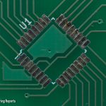
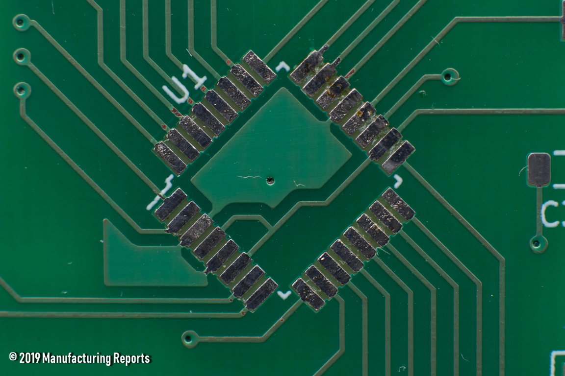
As mentioned above, the HASL surface finish on the PCBs is top notch quality, with a smooth and even appearance across the run. The QFN and QFP footprints are well fabricated as are all the passives down to the 0201.
The slots for the USB footprint were consistently milled with a strong left offset. The design files specify a distance from the edge of the slot to the edge of the pad of 0.25mm. Three boards had the slot milled right against the pad edge, and at best, the distance was 0.20mm. Seeed doesn’t publish a tolerance for plated slots or slots in footprints, but you have to imagine “we’re fine with missing it entirely” isn’t the acceptance criteria.
Copper weight was generally above tolerance with the exception of one board that had a backside copper layer that measured 0.0006″ thick, below even the tolerance for 1/2oz copper.
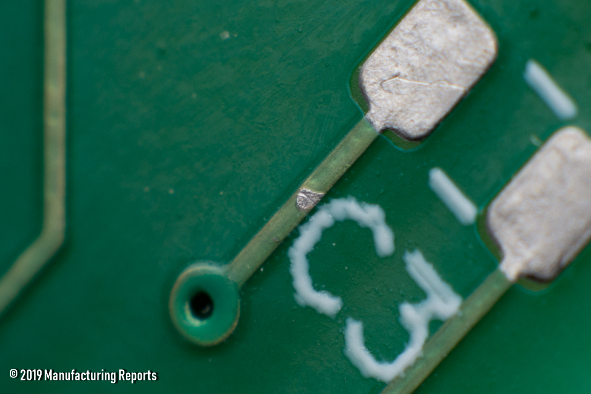
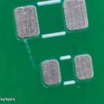
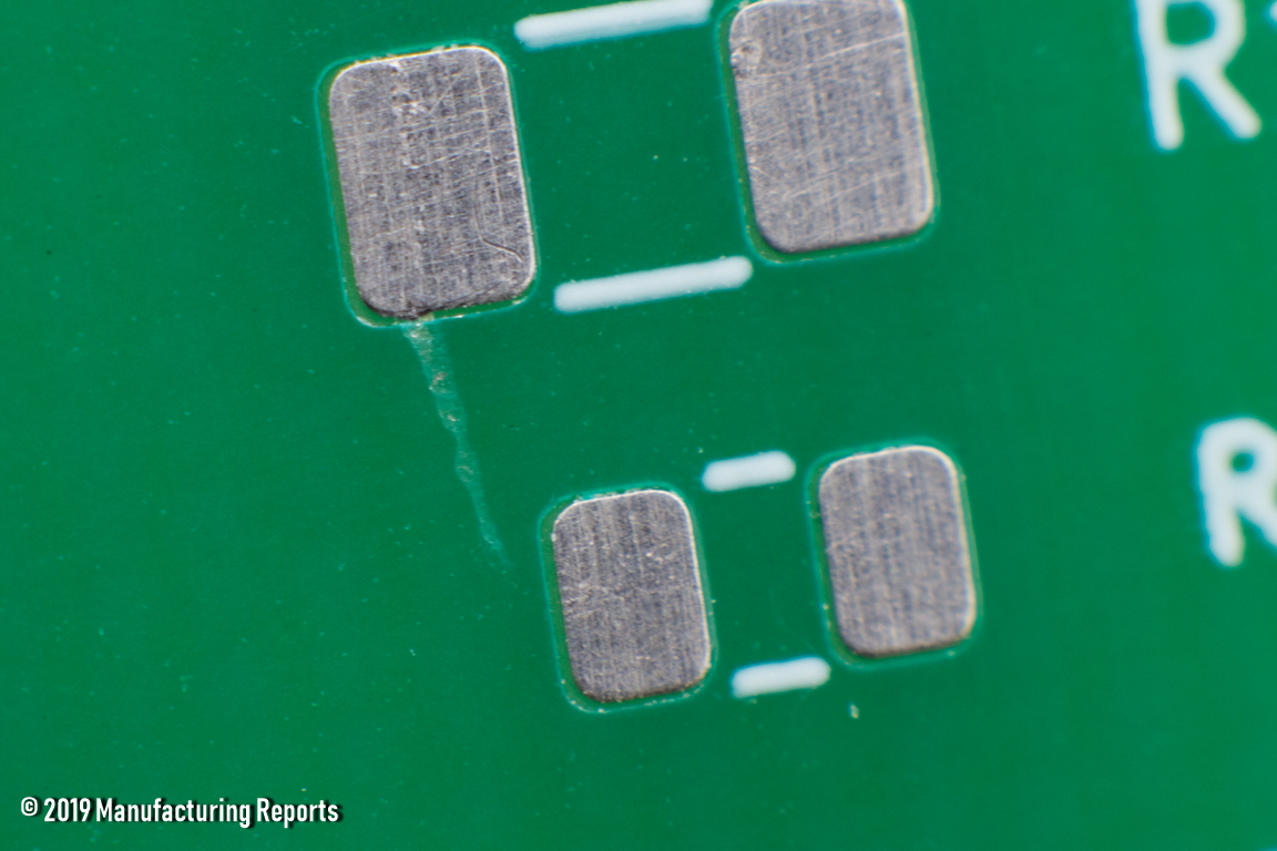
There was substantial trace and via damage on many boards. Some scratches were localized, but some extended across large sections of the board. Some merely marred the surface of the solder mask, while some exposed the trace underneath.
-
- Smooth HASL
-
- HASL on Heatsink
-
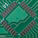
- QFP Footprint
-
- QFN Footprint
-
- 0603 and 0201 Footprints
-
- Distance Should Be 9.8
-
- Damaged Copper Pour
-
- Damaged PTH and Ground Plane
-
- Exposed Traces
-
- Dinged and Exposed Traces
-
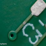
- Scraped and Exposed Trace
-
- Damaged Via
Solder Mask Quality
There were two issues with the solder mask related specifically to the design files I sent. Although these weren’t a problem on any previous board orders, they were oversights on my part (subsequently corrected now in v2.1 of the MRTC which will be the standard).
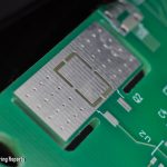
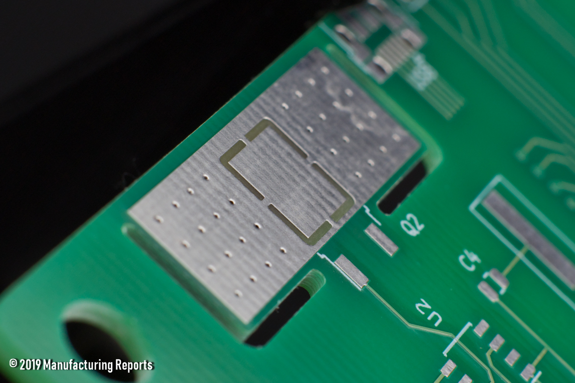
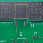
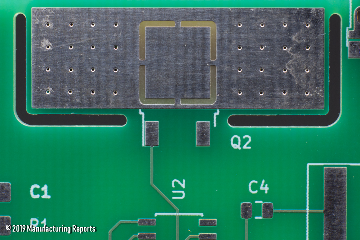
The first issue is that in the solder mask keepout around the copper thickness testing area, I designed the polygon for the keepout and the copper pour to be colinear, while I should have left an offset to make sure the copper ended at a minimum of 4 mil from the edge of the solder mask. 4 mil is the standard I see most regularly, so I measured the amount of ground plane that was exposed and only one board exposed the full 4 mil, others were smaller, with the exception of some blobs of HASL that were stuck to the thin edge of exposed copper pour.
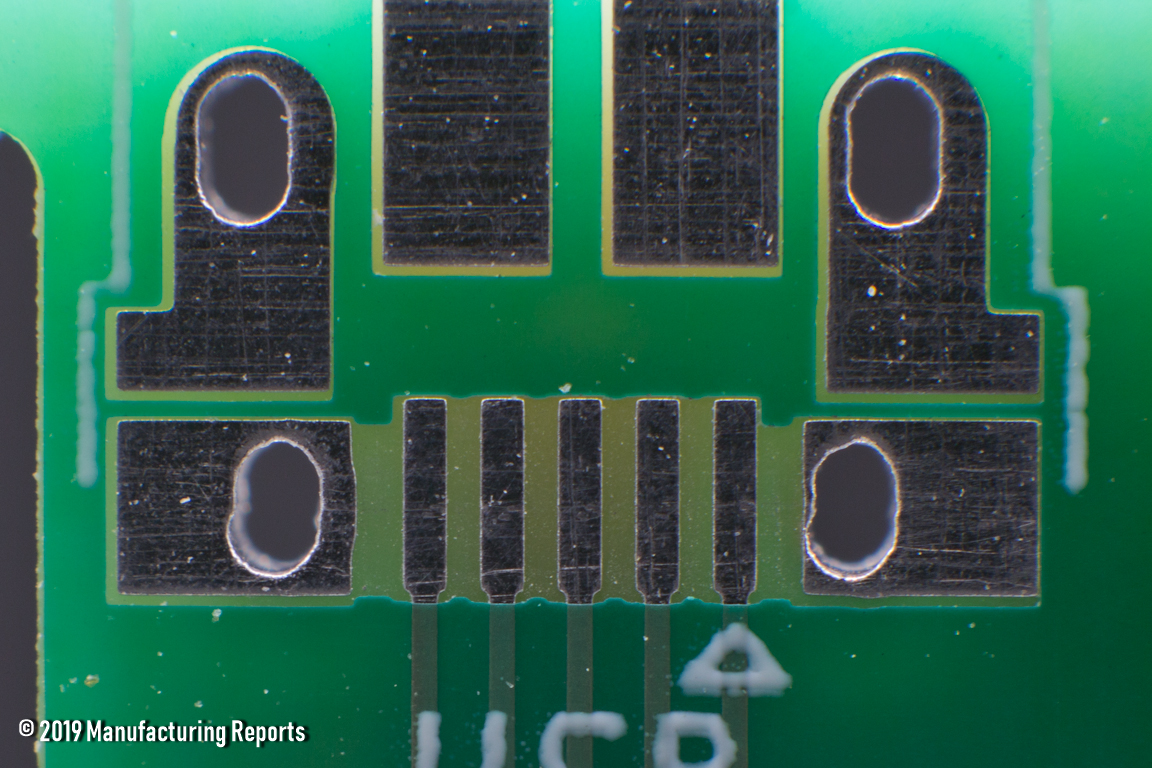
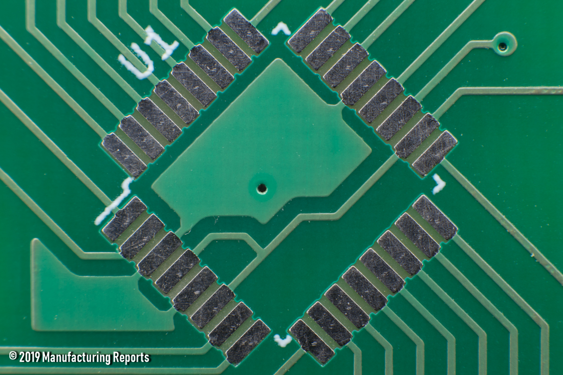
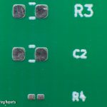
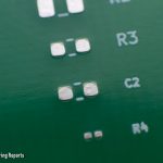
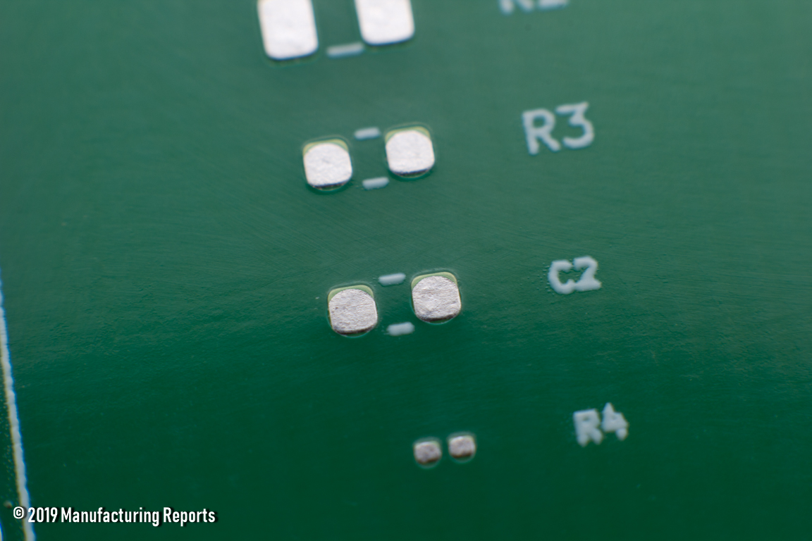
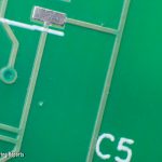
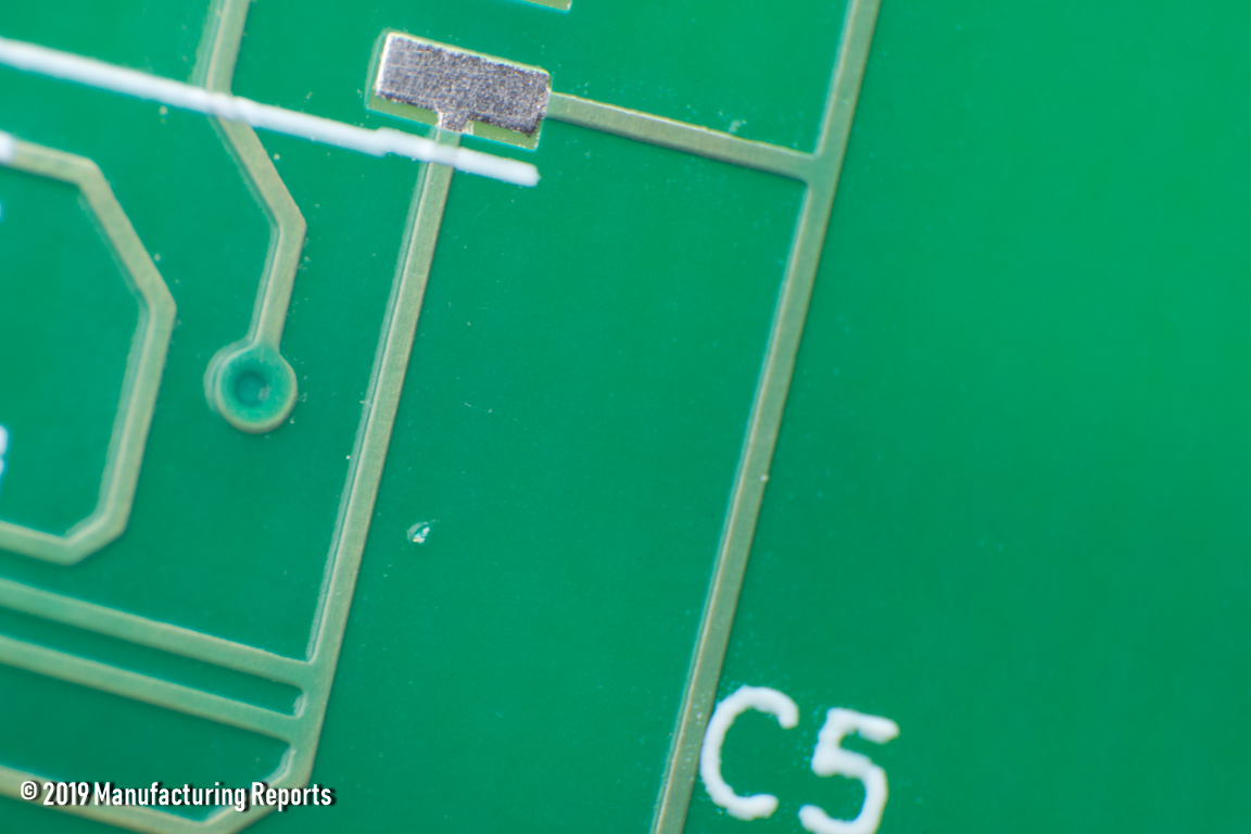
The other issue, is that of the solder mask web or “dam” as it’s sometimes referred. My EDA design rules allow for a web of solder mask between the pads of SMD components of a minimum 6mil / 0.15mm. Unfortunately, (as mentioned above in the Customer Service), Seeed Studio publishes different guidelines on that specification. They impose a minimum width of 12mil / 0.32mm, which excludes solder mask from appearing between the pins of all but the chunkiest of SOIC components. As a comparison, here are the solder mask dam specifications for five other vendors and how they compare with Seeed Studios Fusion PCB service:
| Manufacturer | Minimum Solder Mask Dam (mil) | Minimum Solder Mask Dam (mm) |
|---|---|---|
| ALLPCB | 0.004 | 0.100 |
| OSHPArk | 0.004 | 0.100 |
| PCBWay | 0.004 | 0.100 |
| Shenzhen2U | 0.004 | 0.100 |
| Elecrow | 0.010 | 0.254 |
| Seeed Studio | 0.012 | 0.320 |
Now, beyond those issues, the solder mask is damaged on many boards in various ways. Firstly, it is very thin: the color of the copper is evident on every board as can be seen in many of this review’s pictures.
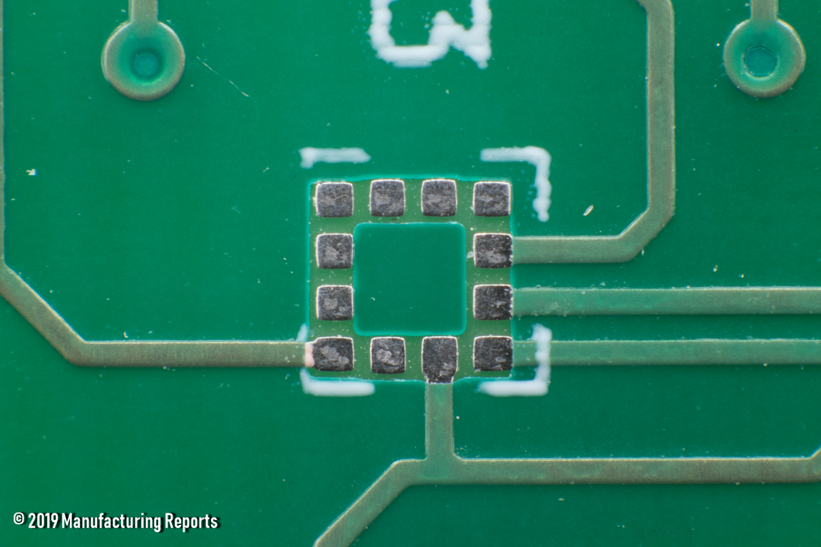
The pads of the smallest passive footprints have had solder mask creep onto the copper, because the aperture seems to have been created too small. This might have been a problem for the QFP and the Micro USB pads, but as stated above, they didn’t put solder mask there.
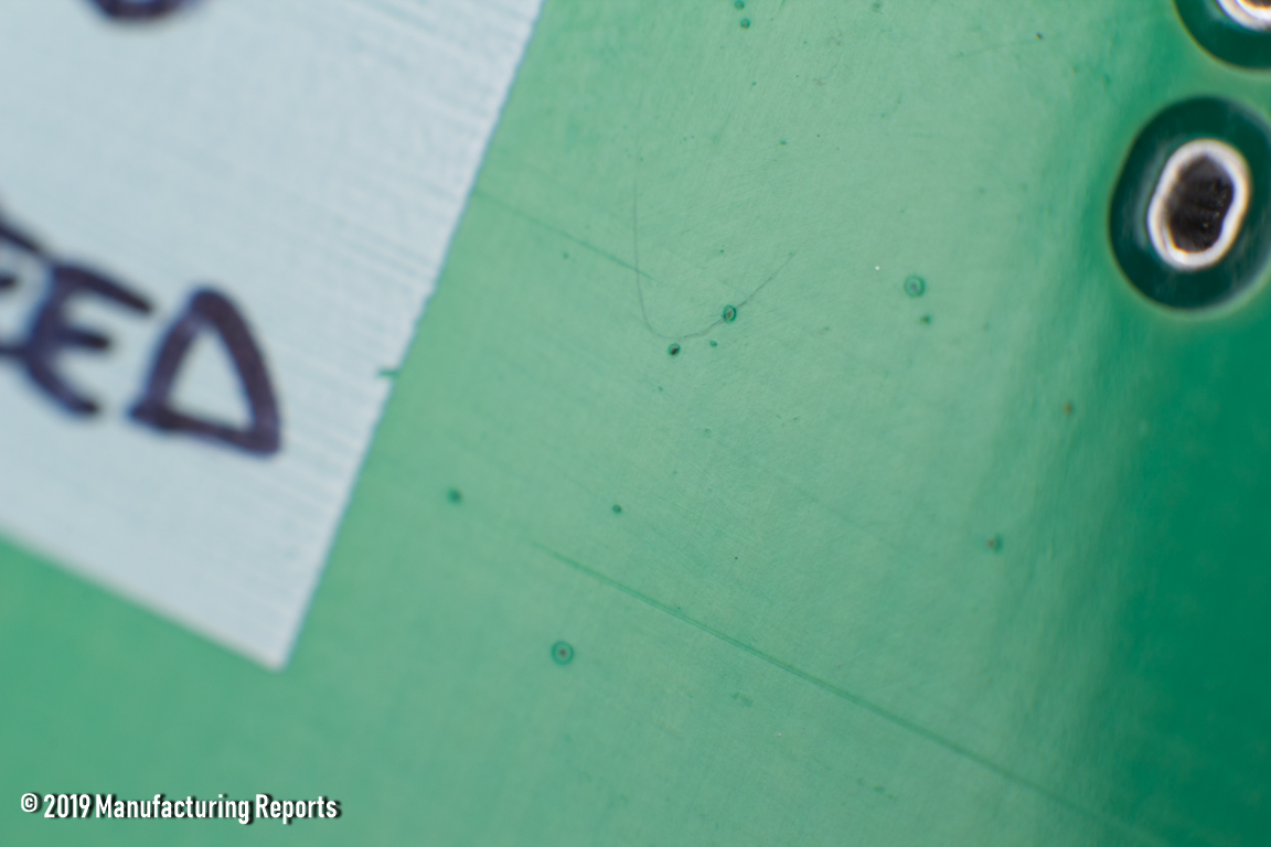
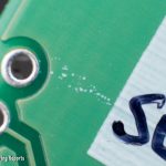
Finally, there is contaminant to be found on the surface and trapped under the mask on several boards as well.
-
- Solder Mask Offset Onto 0603 Pads
-
- Thin and Splotchy Mask
-
- Missing Solder Mask Web
-
- Exposed Ground Pour with HASL Blobs
-
- 4 Mil Exposed Copper Pour
-
- Damaged Solder Mask
-
- White Surface Contamination
-
- Contaminant Embedded in Mask Layer
Silkscreen Quality
The quality of the Seeed Studio Fusion PCB service silkscreen is average. It’s clearly printed using Direct Legend Printing and not through a Liquid Photo Imageable process.
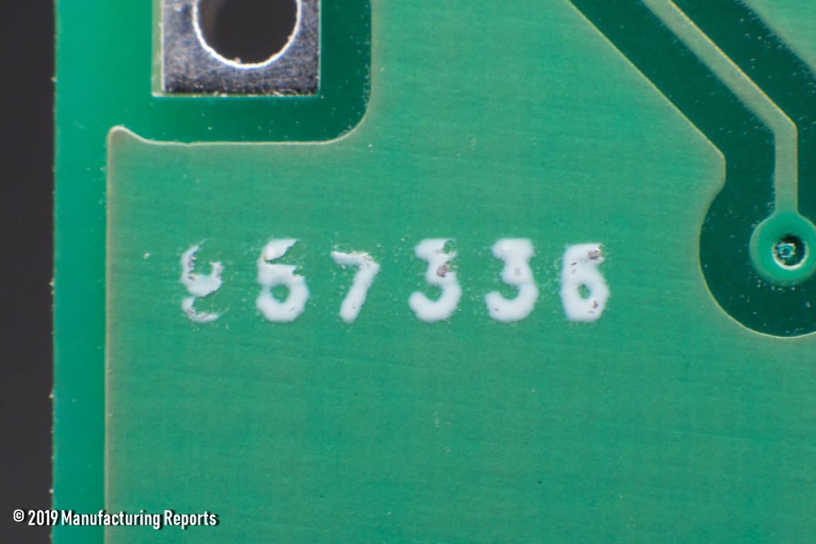
The QR Code doesn’t resolve, but in contrast, the smallest font sizes in the passives area were reproduced with surprising clarity in some cases. There was a small amount of overprint and ink spray, but nothing severe. Reference designators printed over traces didn’t suffer from the varying Z depth.
In a few cases, the front silk layer seemed to get offset during the print process, leaving things a little wonky.
They also printed a manufacturers mark, with no option to relocate it or have it removed.
Generally, the silk is better than some but not as good as others.
-
- Large Font
-
- 0.5 mm Font Size
-
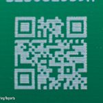
- QR Code
-
- Makers Mark
-
- Print Over Traces
-
- Slight Print Offset
-
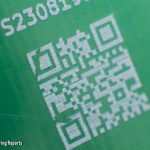
- Scraped QR Code
-
- Silk Overprint
-
- Silk Ink Spatter
Solderability
A board was selected at random and put through the soldering process: the Micro USB Connector and QFP32 were soldered to their pads and then subjected to two rounds of rework.
The QFP sat flat on the footprint before soldering it down, helped by the uniform planarity of the HASL surface finish on the pads. However the lack of solder mask between the pads made avoiding solder bridging difficult and a lot of extra flux and use of solder braid was necessary to clean the joints up, which no doubt caused more abrasion than usual. This may be the cause of the exposed copper through eroded solder mask after merely soldering the QFP down. It is unusual to see those patches there, particularly as they are bare copper. That leads me to suspect that the solder mask erosion occurred during the flux clean up. Clean up is done here at the lab with 99% isopropynol and Kimwipes first to dissolve the remaining flux, then mop it up; no brush is used.
The subsequent two rounds of rework on the QFP32 resulted in significantly more erosion of the resist layer, and I don’t think it would have been feasible to do much more, as the ground pour around the microcontroller footprint was starting to get exposed, and with the difficulty arising from solder bridging, shorting pins to the ground plane was starting to become a possibility.
The Micro USB Connector suffered similarly. It did sit flat on the footprint, but soldering was a mess of bridging again, requiring the use of braid and extra flux, and some erosion of the mask layer can be seen extending from the pads, although bare copper isn’t present as it was with the QFP32. The rework rounds degraded the mask layer further, nearly obliterating the “USB” reference designator, and extending up the traces by as much as 2.5mm.
None of the pads lifted, and the solder mask and silk layers didn’t discolor from the hot air rework, although the silk screen by the micro USB did suffer damage.
-
- QFP32 Before Soldering
-
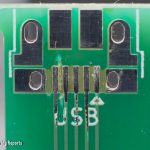
- Micro USB Before Soldering
-
- QFP32 After Soldering
-
- Micro USB After Soldering
-
- QFP32 After Rework Round 1
-
- QFP32 After Rework Round 2
-
- Micro USB After Rework Round 1
-
- Micro USB After Rework Round 2
-
- QFP Post Rework Closeup
-
- Micro USB Post Rework Closeup