Elecrow PCB Review
Elecrow PCB
Shenzhen, China
$2.09
1 Day
1 Day
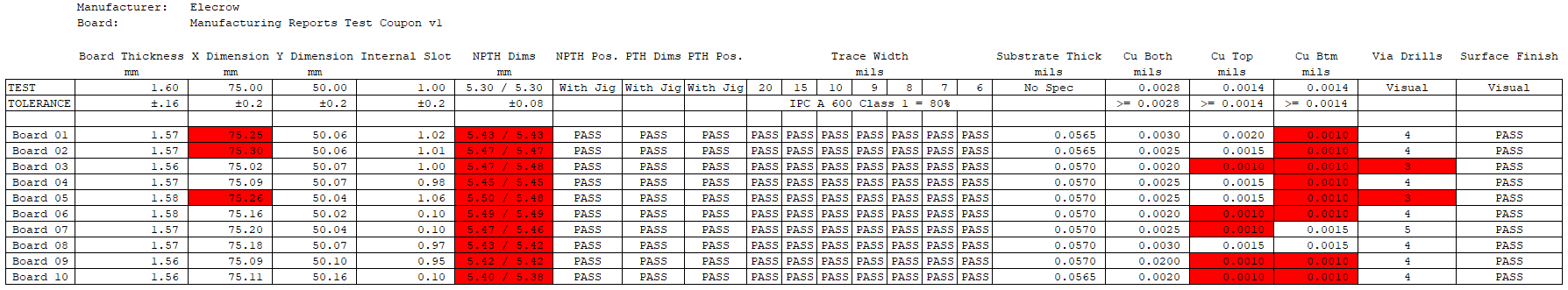
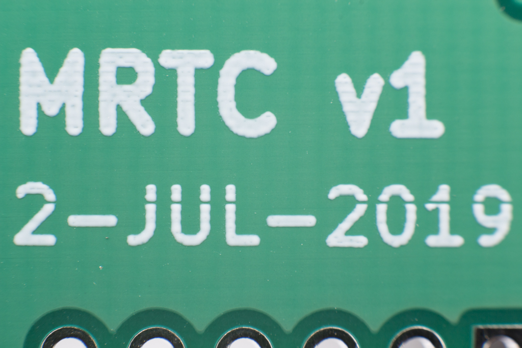
Manufacturing Reports Test Coupon v1
Excellent HASL
Clean Solder Mask with Little Contamination
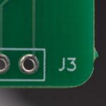
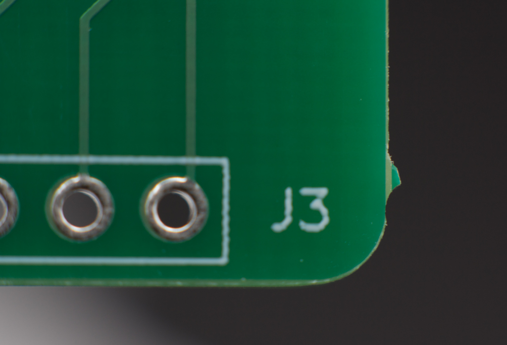
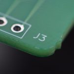
Good Quality Silk Screen (still DLP though)
Poor Edge Cuts
Lead-in/Lead-out Marks on Milled Edges
1oz. Copper Thickness Below Tolerance
Illegible Invoice
I’ve used them for production runs in the past and had good boards spun, so I was hoping to have the same experience sending out the Test Coupon for this Elecrow PCB Review. They are another PCB Manufacturer and EMS located in Shenzhen, so competition for quality and cost is fierce.
Cost
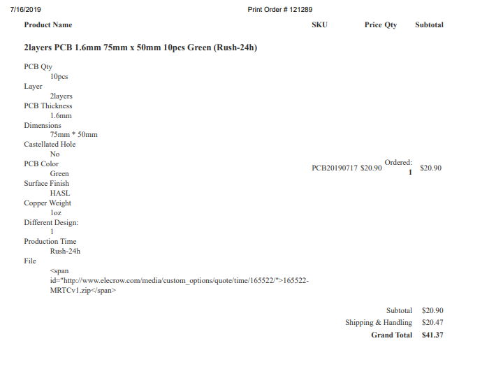
Elecrow is at the higher end of the low cost offshore manufacturing spectrum, with a final cost of $35.43. for 10 copies of the Manufacturing Reports Test Coupon. That broke down to $2.09/unit with an additional $20.07 for expedited DHL shipping. There were no additional fees or markups for either the payment processing or shipping.
Ordering
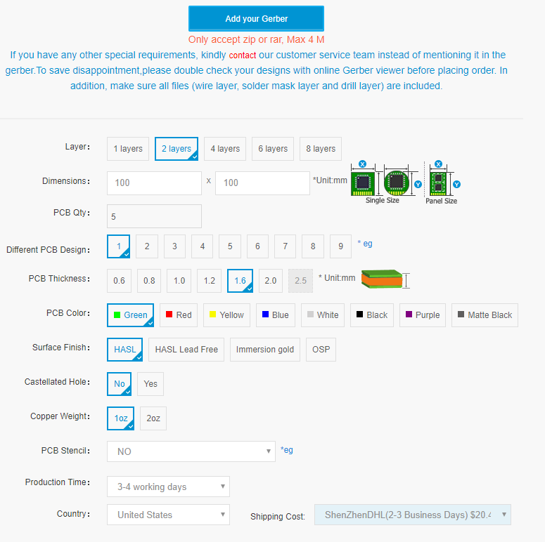
Under the big retail product slider on the main page, is the “PCB Services” link, and that takes you to the standard board stackup interface familiar to anyone who has used Chinese board fabs. This review covers the standard PCB service.
Standard service time is 3-4 working days, with 48 and 24 hour turn service available at a $5.00 and $16.00 additional cost respectively on an order of 10 boards. More boards and larger dimensions raise the rapid turn premium. I settled on the default board options and selected the 24 hour rapid turn.
Design Rules were somewhat difficult to obtain, as the top link in a google search returned an HTTP Error 500. On the order page, however is a link to a PDF file titled “PCB Specification && FAQ“, which contains the acceptable dimensions.
I was curious about their “Purple” PCB option, since I’m assuming it’s a direct attempt to look like the boards OSH Park ships, and it turns out boards with that solder mask are only produced on Tuesdays and Friday and raise the standard service price from $4.50/10 boards to $24.90/10. That was a little too rich for my blood to explore a whim.
Gerbers were uploaded, stackup selected, and boards added to the shopping cart, which required the creation of a login on the Elecrow website. The checkout page was straightforward but did include an area that asked if I had any “extra demands”. I thought about asking for a drawing on the shipping container, but then settled down and requested that they note a PO# on the invoice. No gerber preview or board render is presented.
There was no option to prevent printing of a manufacturer’s mark in the silkscreen, however once the boards arrived, none appeared.
Placing the order opens up the PayPal page, and after submitting payment, you’re sent back to Elecrow for your order confirmation number, and a rather poorly formatted document. The main problem with this is that in a business process where you as the engineer need to submit this with an expense report, this creates an extra layer of hassle. Filing expense reports is always a pain at the best of times, even without garbled or confusing payment documentation from a manufacturer.
-
- Checkout Page
-
- Order Confirmation
Fulfillment
Two days after submitting the order I received a text message from DHL with a tracking number and showing an estimated delivery date. However an email from Elecrow didn’t arrive until two days later, which was a little odd, but one way or the other, their work flow notified me of the inbound shipment and the tracking number. Eventually.
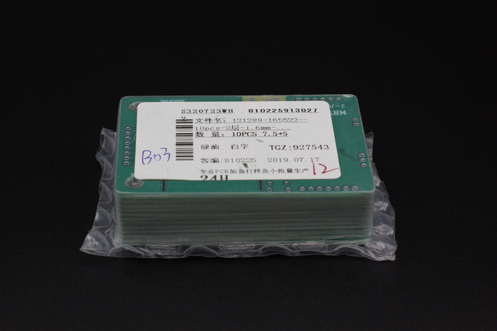
The order arrived in a typical DHL envelope, inside of which was a simple, unbranded cardboard box with the order number written on the outside in marker pen. The box contained the boards, vacuum sealed in a bubble pouch and wrapped in more bubble wrap, with a copy of the invoice (including PO #).
Against our order of 10 boards, 12 were shipped.
-
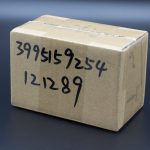
- Shipping Box
-
- Order Packaging
Customer Service
Elecrow publishes EagleCAD design rules as well as standardized design rules for other CAD packages.
Obtaining a copy of the invoice from their site was problematic. It required digging into the My Account section of the site and ultimately produced a garbled PDF.
An email was sent to their “Logistics” email address explaining the problem and asking for a PDF to be emailed, and I received a clean copy within a day.The PO# I requested as an “extra demand” during the order process appeared on that invoice.
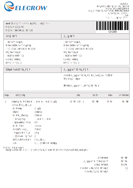
Elecrow Garbled Invoice
Circuit Board Visual Inspection
-
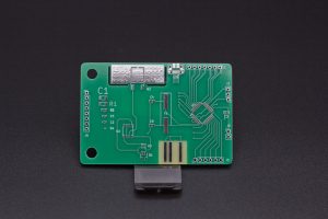
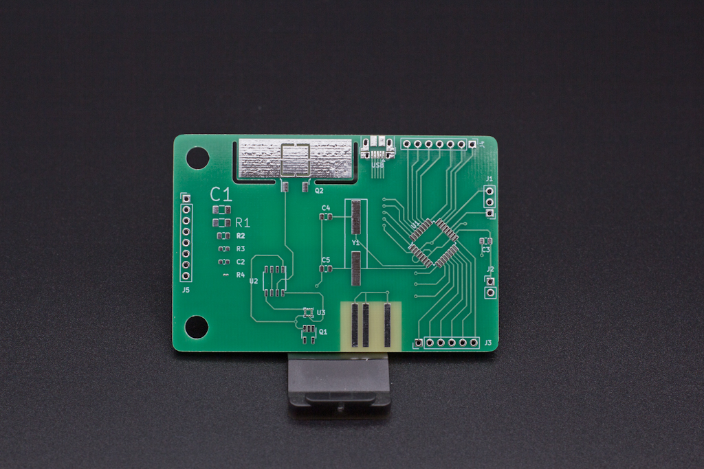
- Elecrow Full Board Front
-
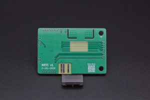
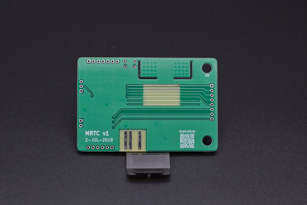
- Elecrow Full Board Back
The boards have typical green solder mask, and HASL finish as requested in the ordering options at checkout. During the initial visual inspection I was struck by how beautifully uniform the HASL looked on some of the boards, almost as though it was plated.
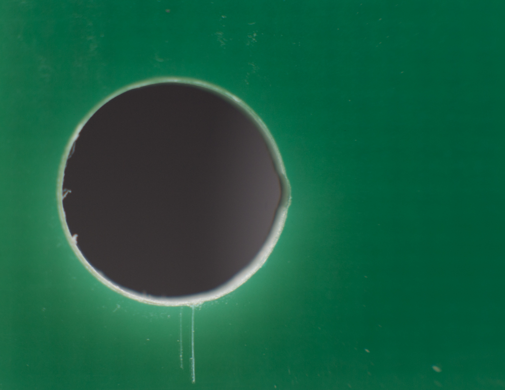
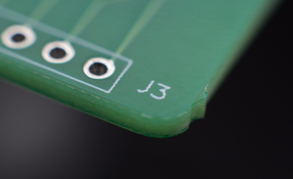
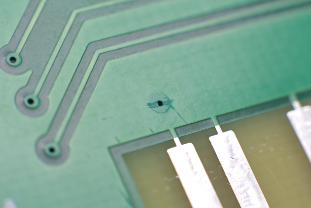
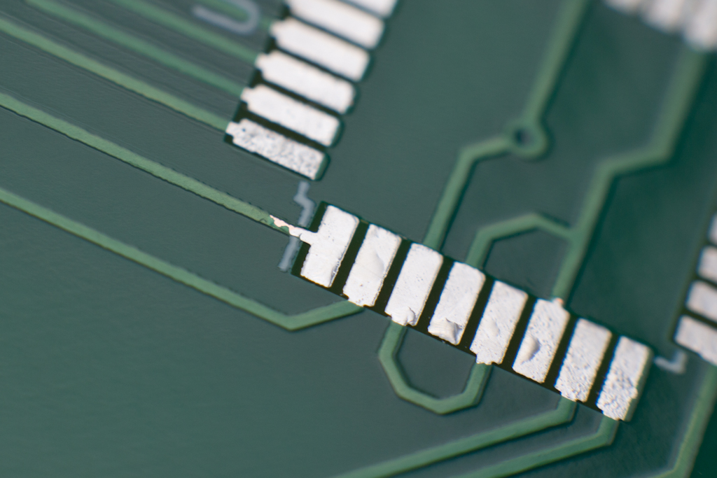
The board edges featuring lead-in/lead-out witness marks on the edge from the milling process, that resulted in a raised boss in three cases. There were witness marks in the mechanical holes from their fabrication as well.
At first glance, the HASL over the heat sink area looked very clean and even, as did the solder mask over the via stitching in the back.
There was a slight amount of milling dust that had to be wiped off the boards after removing them from the order packaging.
PCB Dimensions
The milled dimensions on the board were severely skewed by the lead-in/lead-out marks that appeared in the board outline and the milled NPTH mechanical hole. On the three boards with a raised boss on the outer edge, the boards failed the outer dimension tolerance measurement, being 0.3mm oversized in one case.
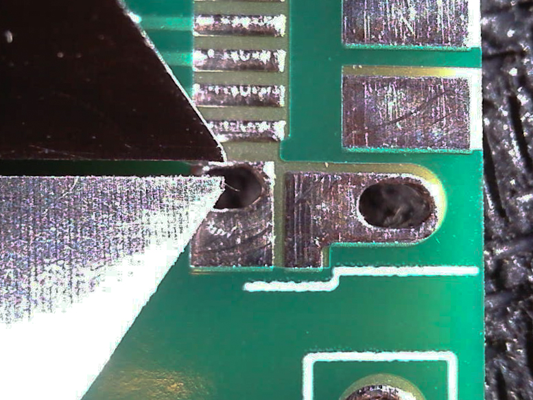
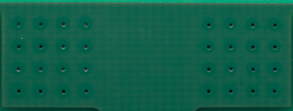
The mechanical NPTHs were universally over sized out of tolerance due to the lead-out notch, as it featured in each NPTH on each board, although positioning matched well with the NPTH test jig.
Plated through hole sizes and positioning passed well compared against the PTH test jig. The mechanical slot around the heat sink measured within tolerance as well.
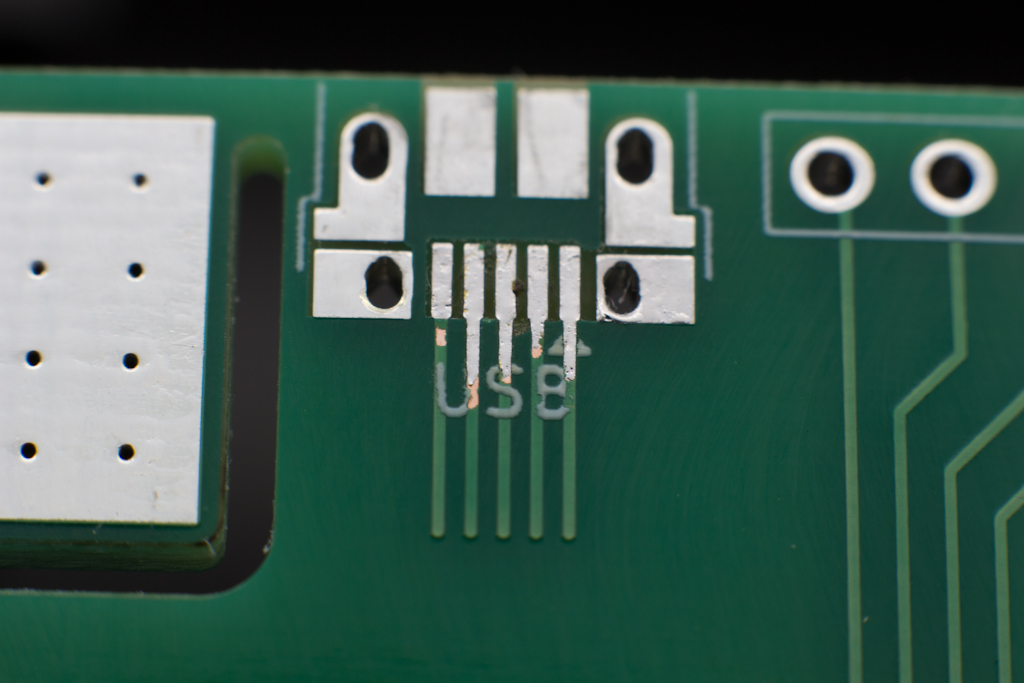
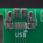
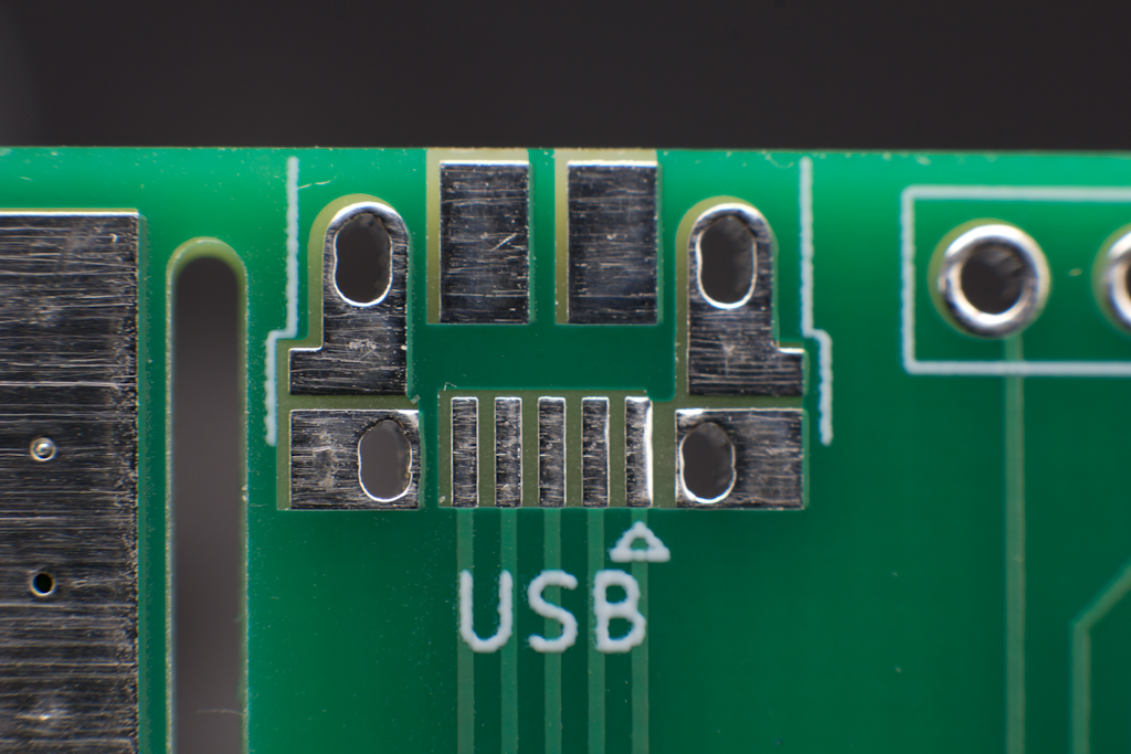
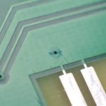
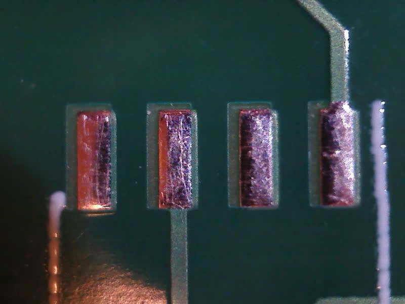
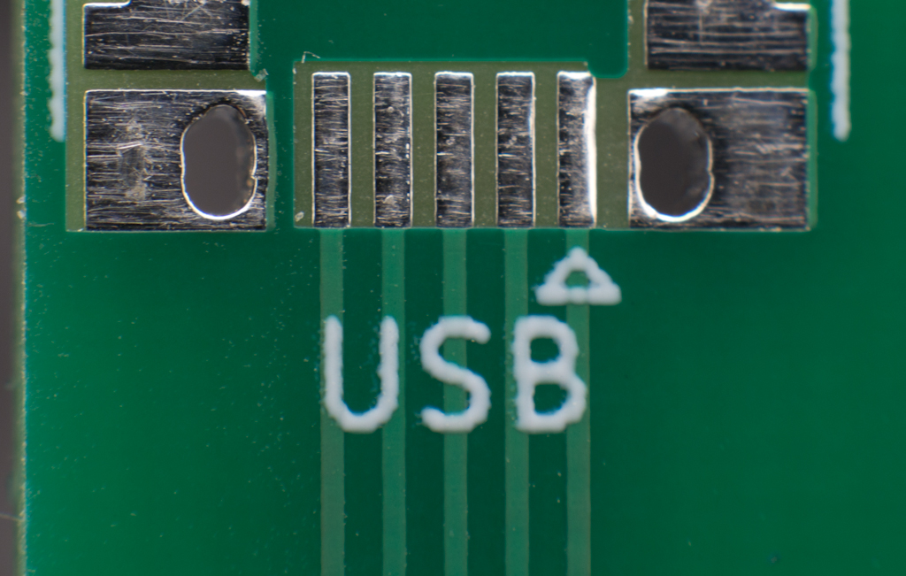
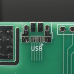
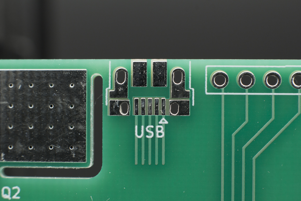
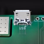
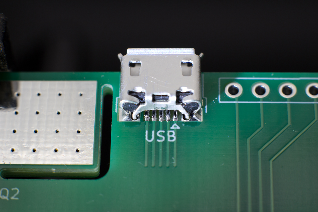
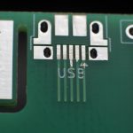
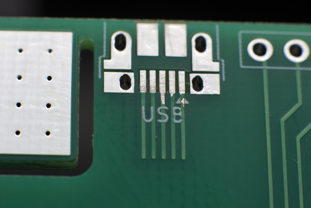
The plated slots on the USB connector were relatively straight, however they did come dangerously close to the pad edge. In the included photo below, the calipers are measuring the correct distance from the pad edge where the slot should appear.
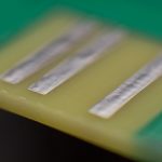
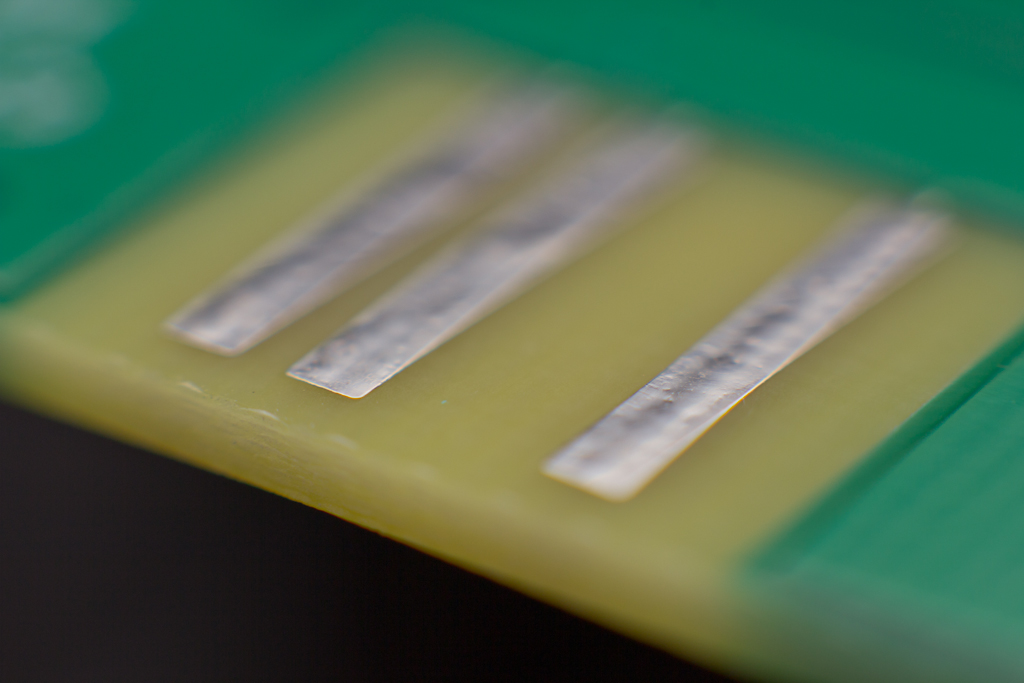
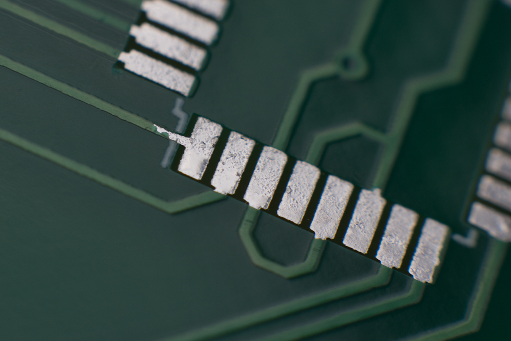
Trace widths were all well within tolerance, although some traces were undersized by 1 mil on several boards.
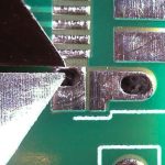
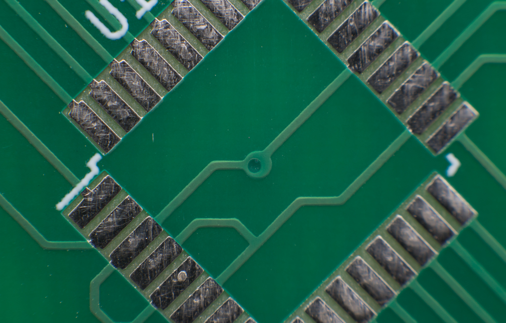
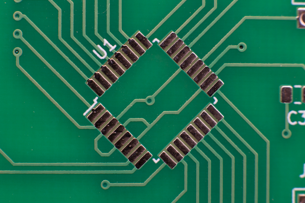
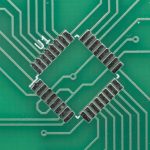
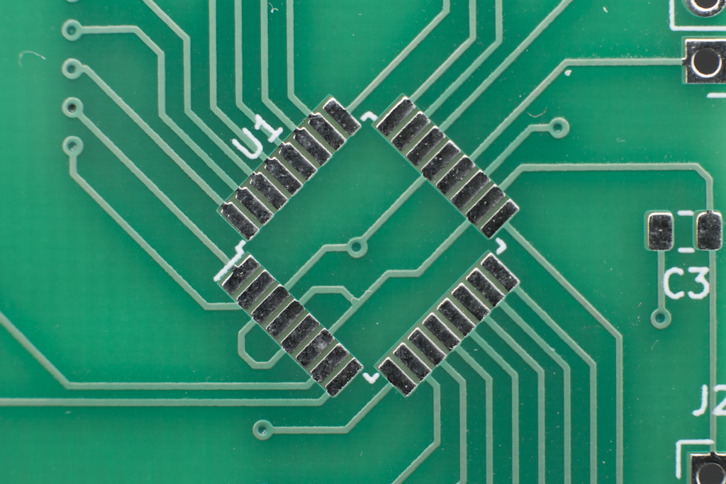
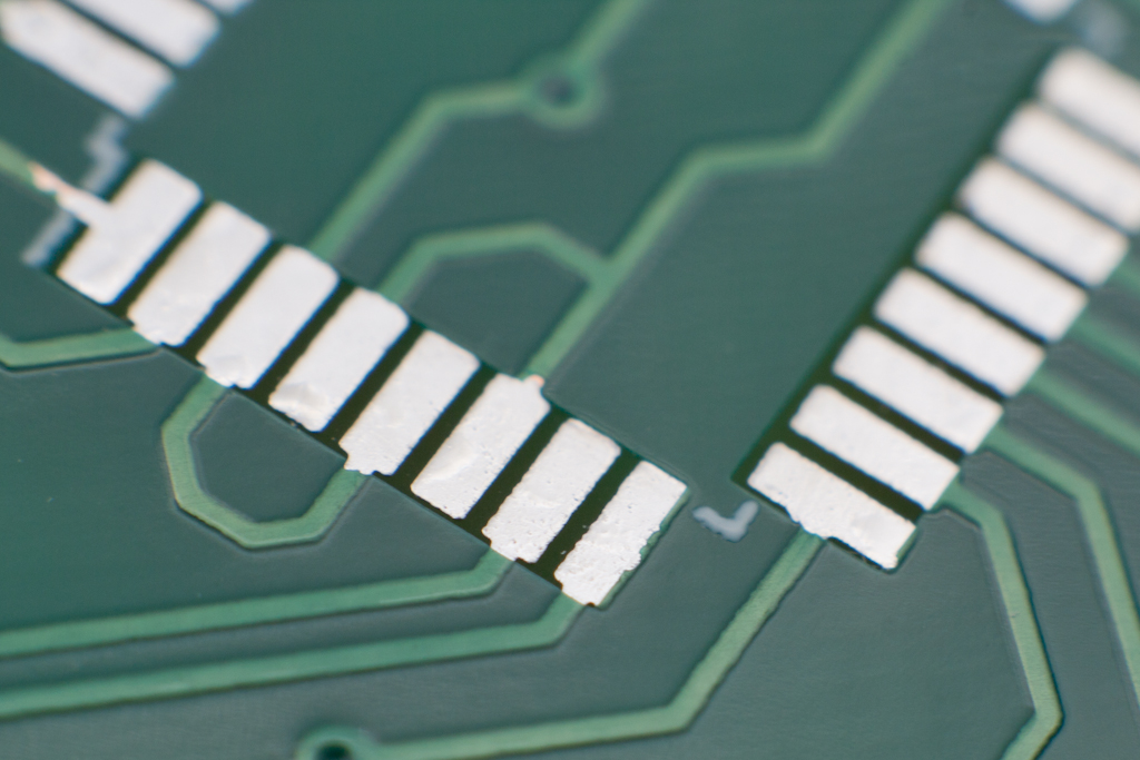
With the exception of one board, all the via drills were offset from center, and in two cases were hazardously close to the via edge.
Elecrow Test Report 2019
-

- Witness Mark in NPTH
-
- Bad Milling of Board Edge
-
- Raised Boss on Board Edge
-
- USB Plated Slot Offset
-
- Plated USB Slots
-
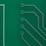
- Typical Via Drill Offset
-
- Via Drill Offset in QFP
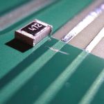
Copper Layer Quality
The copper weight on all but one board measured below tolerance. The measurements were so low, in fact, that I verified the measurements three times across each board. Combined with the slightly smaller trace widths on some boards, the thin copper could be hazardous when it comes to an application that requires carrying any real current.
One board had the solder mask completely scratched through exposing the trace underneath which tested conductive to the pad at the end of the trace net. On another board a via was significantly scuffed / scratched.
The HASL on these boards, however, is exceptional. There is a uniformity and consistency across the boards that is unique, appearing in some cases to look plated for all it’s smooth surface finish.
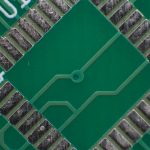
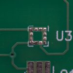
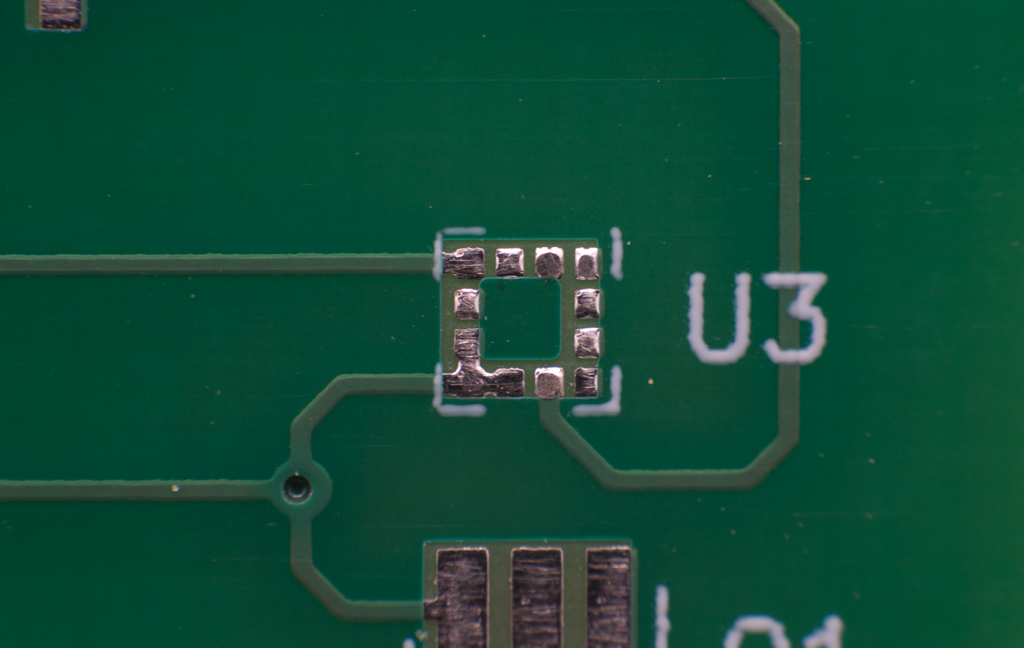
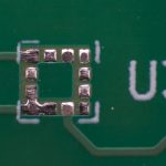
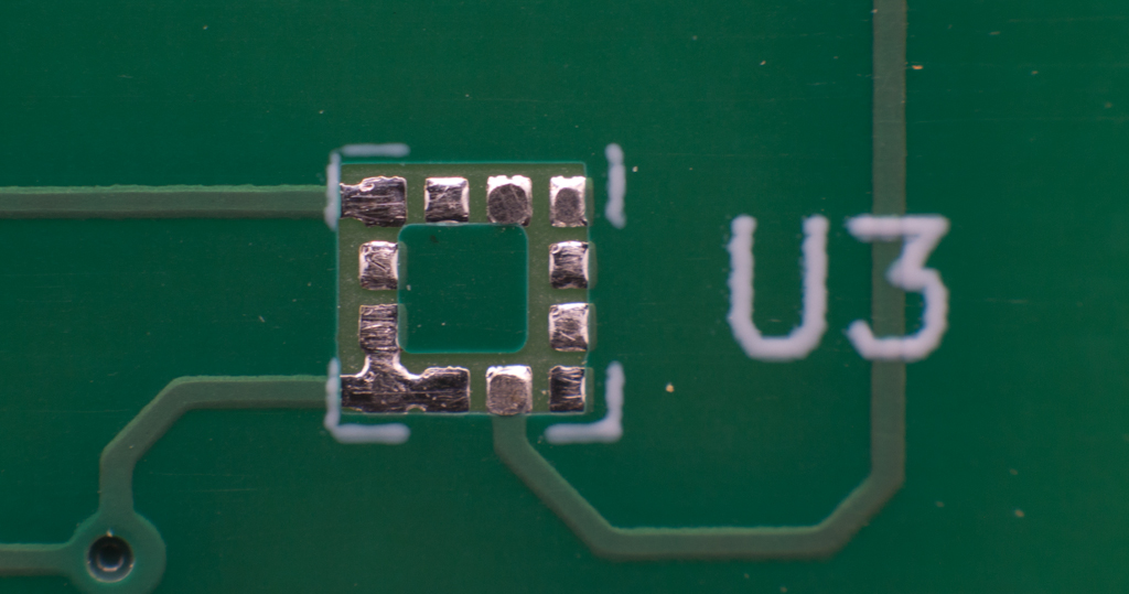
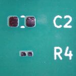
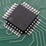
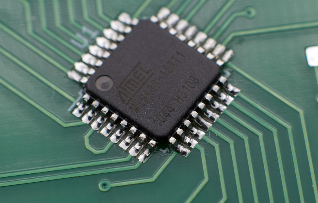
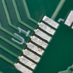
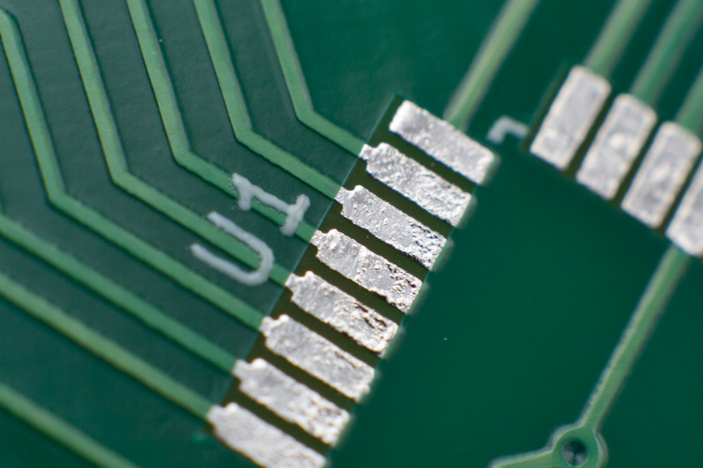
The QFN and QFP footprints were both very well fabricated across all 10 boards. The passive footprints were all clean and usable.
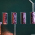
The plated slots in the USB connector were quite rough looking, if relatively straight as mentioned above. While the slots had a very rough, uneven, appearance under magnification, the USB connector did fit into each board successfully.
-
- QFN Footprint
-
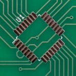
- QFP Footprint
-
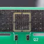
- Heatsink HASL Surface
-
- Copper Thickness
-
- Damaged Trace
Solder Mask Quality
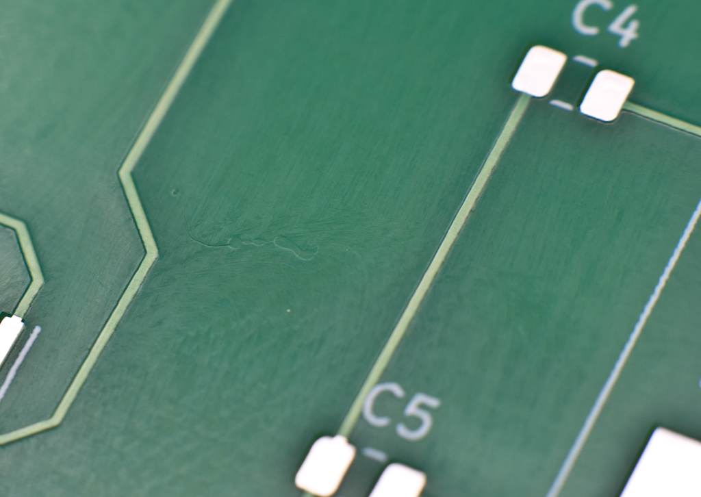
The solder mask over the heat sink via stitching is well applied. It appears consistent and even with no sign of wicking or sinking into the vias at all. Only one board showed any contamination trapped under the mask, and no boards showed contamination on the surface.
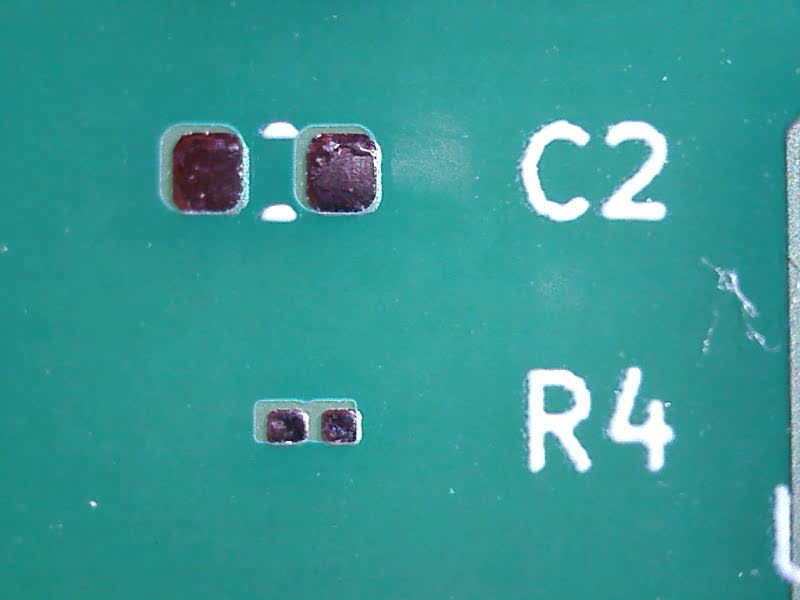
On four of the boards, the mask offset was sufficient to drive the ink onto the pads of the SMD components.
-
- Solder Mask Offset QFN
-
- Solder Mask Offset Passives
-
- Solder Mask Contaminant
-
- Solder Mask Over Via Stitching
-
- Damaged Via
-
- Solder Mask Offset SOIC-8
Silkscreen Quality
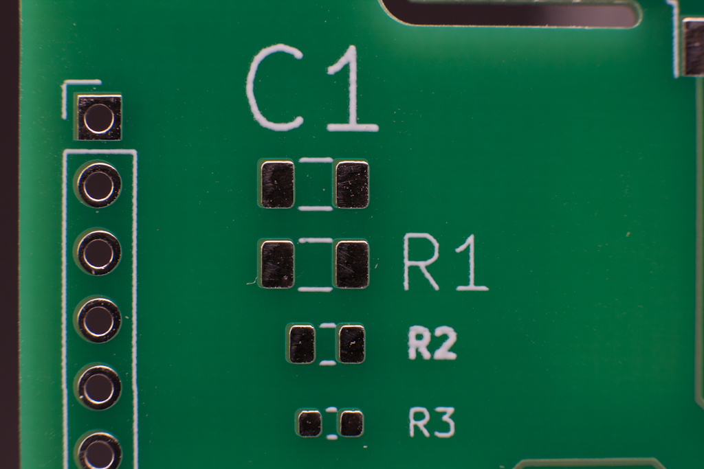
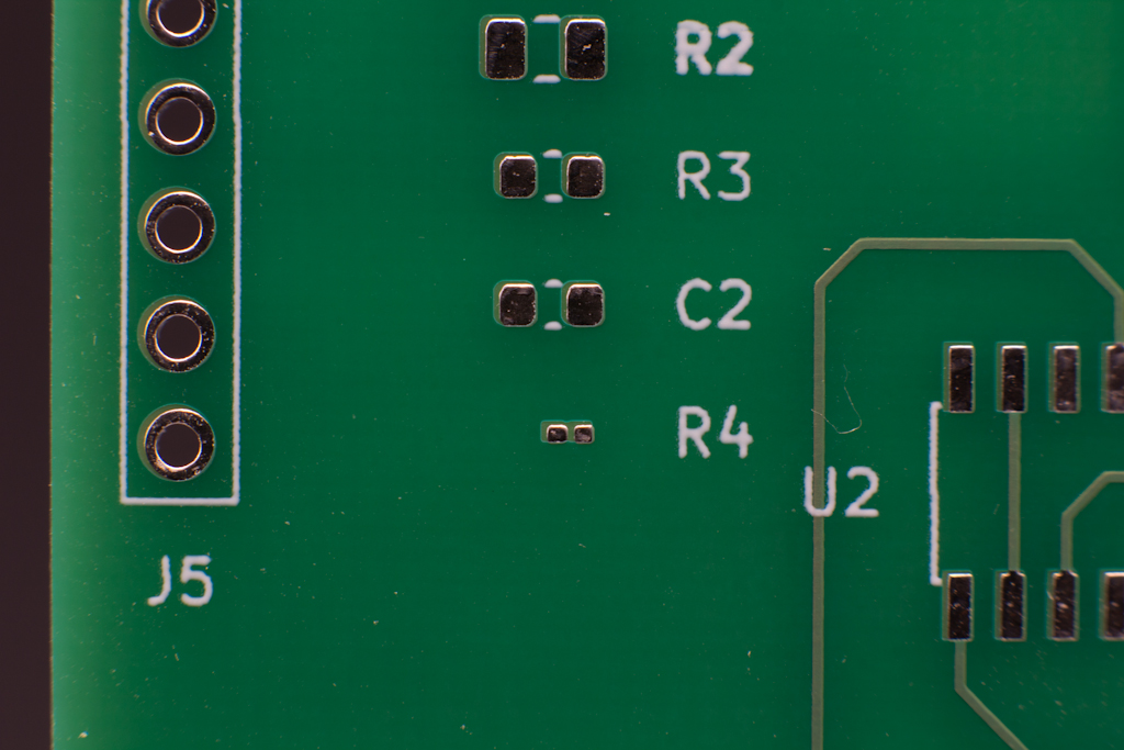
While the silkscreen layers are created using the direct legend printing method, it is some of the best direct printing I’ve seen, with no problems or printing gaps when crossing over traces (having thinner than expected copper probably helps). The various font sizes all resolved well in the passives footprint area, and all reference designators were legible.
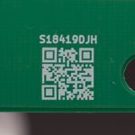
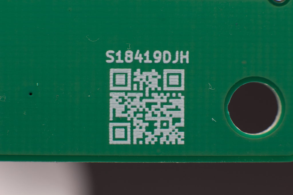
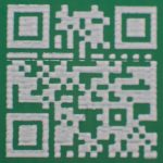
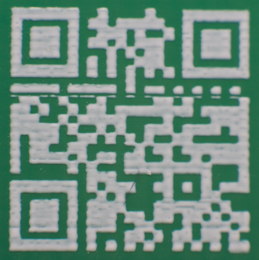
All 1cm QR codes were readable with magnification, and in some cases, even without, with very crisp 90 degree corners in the QR artwork.
The only significant issue was a blank line that appeared on the back side silk layer towards the bottom of the board, passing through the date under the board name and across the QR code on five boards.
-
- Crisp Reference Designators 01
-
- Crisp Reference Designators 02
-
- QR Code Resolution
-
- Clean Silk Over Traces
-
- Gap Through Date Code
-
- Gap Through QR Code
Solderability
The QFP32 and Micro USB connector were soldered onto the board with little trouble. Both components matched their footprints well and sat flat on the PCB.
The USB connector was removed easily through rework. The solder mask on the traces leading to the pads started to suffer and had crept back after clean up was finished, with significant signs of mask erosion occurring after the second rework cycle. (In the pictures below, a second board was necessary to document the rework of the connector as the first pictures were corrupted in the camera).
The QFP32 footprint demonstrated very little erosion of the solder mask or pads during the two rework cycles, with only marginal solder mask removal occurring on one pad. Solder removal with braid was easy and left clean pads for rework.
The silk screen around both footprints showed no adverse affects from either initial soldering, rework or clean up with 99% isopropynol, beyond the solder mask deteriorating beneath it.
-
- QFP32 Presolder
-
- Micro USB Presolder
-
- QFP32 Post Solder
-
- Micro USB Post Solder
-
- Mask Erosion After Rework 01
-
- Mask Erosion After Rework 01
-
- Mask Erosion After Rework 02
-
- Mask Erosion After Second Rework
-
- USB Connector After First Rework Cycle
-
- USB Connector After Second Rework Cycle