PCBWay PCB Review
PCBWay
Shenzhen, China
$0.50
1
1
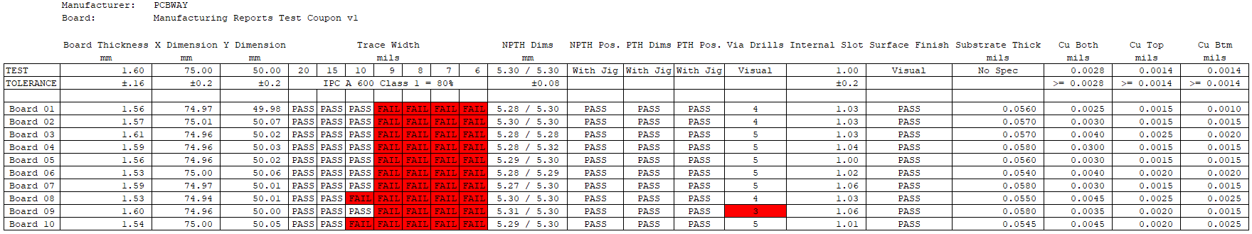
Manufacturing Reports Test Coupon v1
Excellent Fulfillment
Quality Customer Service
Good Solder Mask Quality
Significantly Offcenter Via Drills
Trace Widths Below Tolerance
Quick Erosion During Rework
PCBWay has been winning the word-of-mouth advertising game for both their PCB Fabrication and Assembly services. Many engineers I’ve spoken with have given glowing assessments of how remarkable it is to be able to order boards for pennies and have them delivered with express shipping, so it was obvious to me it was time to write a PCBWay PCB Review of their prototyping service.
Cost
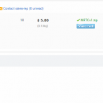
PCBWay is a budget service, coming in only a few dollars more expensive than non-discounted JLCPCB (review of their PCB service here) at $24.00 even. The cost of the boards was $5.00 total for 10 copies of the Manufacturing Reports Test Coupon, and then an additional $17.00 for DHL and then some enigmatic $2.00 “Bank Fee”. I’m assuming that’s passing the PayPal transaction cost back onto me, but random unexplained fees are never encouraging. That $17.00 looks suspiciously like $16.81 rounded up to the nearest whole dollar, which is what I was charged at JLCPCB for basically the same shipping service. So essentially, less some rounding and bank fees, the cost is exactly the same.
Ordering
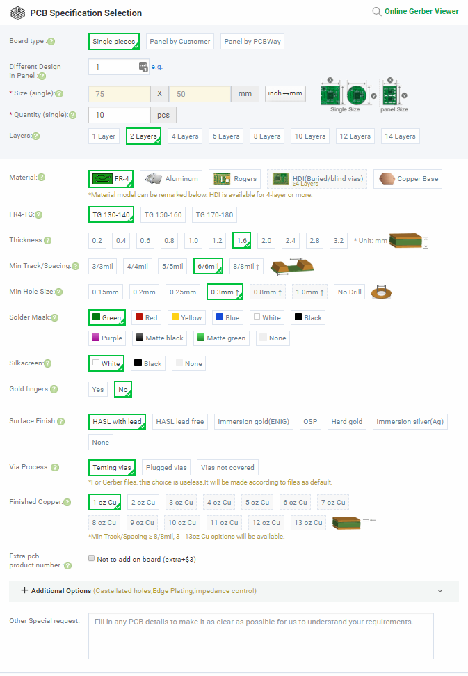
The PCBWay order page presents two important choices right up front, Standard PCB and Quick Turn PCB. The only readily available information on the PCBWay site I could find explaining the difference was a single line: “The PCB manufacturing time is shorter than advanced PCB.” The ordering options available between the two services is very different, with fewer being available for Quick Turn, which makes sense. For example, copper thickness on the Quick Turn page offers 1oz, 2oz and 3oz copper, where as on the Standard page you can order from 1oz to 13oz copper in 1oz increments.
Design Rules for PCBWay fabrication are easily found on their “Capabilities” page.
There were two options that I found particularly interesting. With both services, there is an option (at a $3.00 premium per order), to not have a fab house production number stenciled onto the board. Having these weird fab numbers appear in the silk screen is something I specifically look for when reviewing boards, so it’s nice to see a fab offering a solution for it, even if it costs extra.
The other option is under the Quick Turn page: they offer you the option of having the UL Logo added to silk, mask or copper layer. Something about that just seems odd to me.
Defaults were selected using both service pages and both ended up with the same 24 hour service, with 3-5 day DHL. Somewhere in their business logic there would probably be a cutoff where board orders of a certain stackup go to a different factory and result in longer lead times, but I didn’t dig too deep into the options to find out what those cutoffs were.
After uploading gerbers during the order process, PCBWay immediately performs some kind of validation on the design files, and the Checkout button is grayed out until that review is completed on their side. If you’re wondering how long that review takes, they say towards the top, “We will finish review of your order in 1 hour or less 10 mins.”
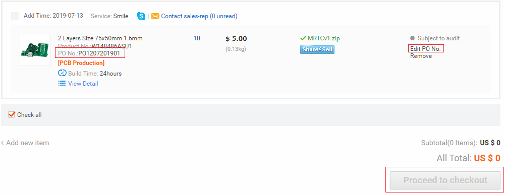
A nice feature of their order status page is the option of adding a PO # to the order, so I added one to see where it would appear during the processing of the order.
Sometime later, the design was approved and I proceeded to payment. A proforma invoice was presented right away, but unfortunately, Amex isn’t allowed as a direct payment method, so I had to go with PayPal. The payment is just as fast, but some previous employers have given me grief when trying to expense PayPal receipts, particularly ones that list the seller’s info exclusively in Chinese characters, so be aware.
At no point was I shown a preview of the fabricated board, so items such as the milled slot around the via stitched heat sink would be a mystery to determine if they’ll be fabricated. If this were a production board I was ordering, and not the Test Coupon, I would definitely contact customer support before payment though.
-
- Standard PCB Service Ordering Options
-
- Checkout Page
Fulfillment
Waiting for the order was non-eventful, with the order page updating to show the status of the production, and an email being sent with the DHL tracking number.
The order was shipped in a standard DHL bag, with a cardboard box inside that was filled with padding. The boards were bundled together inside a vacuum sealed padded pouch.
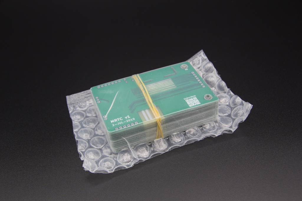
PCBWay Order Packaging
Customer Service
After placing the order, I noticed that the paypal account had an old shipping address in it, so I had to send a real support email, instead of the usual test email, to confirm that the correct address was used. A response was sent around 12 hours later, that seemed to indicate everything was going to be okay. While their customer support staff’s command of English isn’t 100%, it’s certainly far better than my non-existent Mandarin.
The account management pages on the PCBWay website are easy to navigate and provide a lot of detail on order status, past orders, invoice downloads and address book management. This is in contrast to many sites that are more bare-bones and only provide a basic table with the order number, cost paid and the word “pending” until the order ships, and the only account management allowed is a password change.
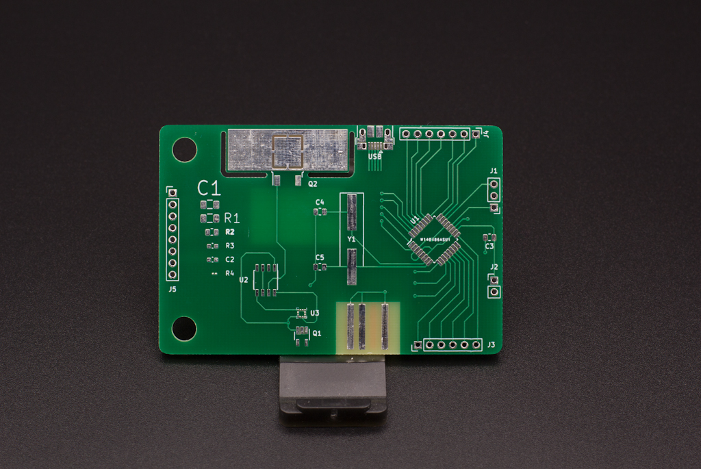
PCBWay Review: Circuit Board Visual Inspection
-

- PCBWay Full Board Front
-
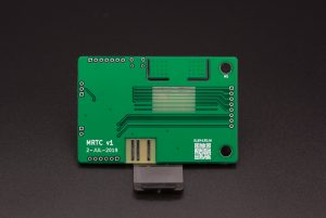
- PCBWay Full Board Back
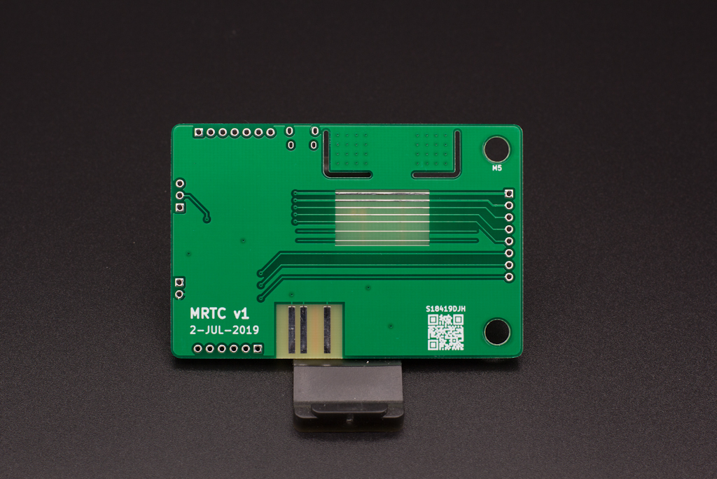
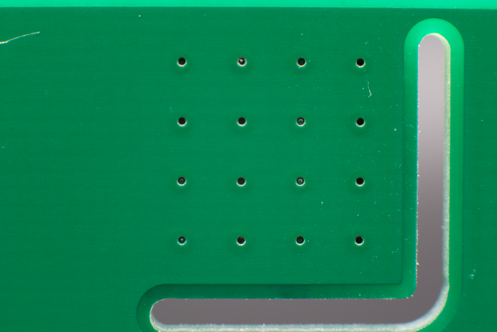
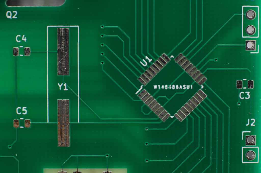
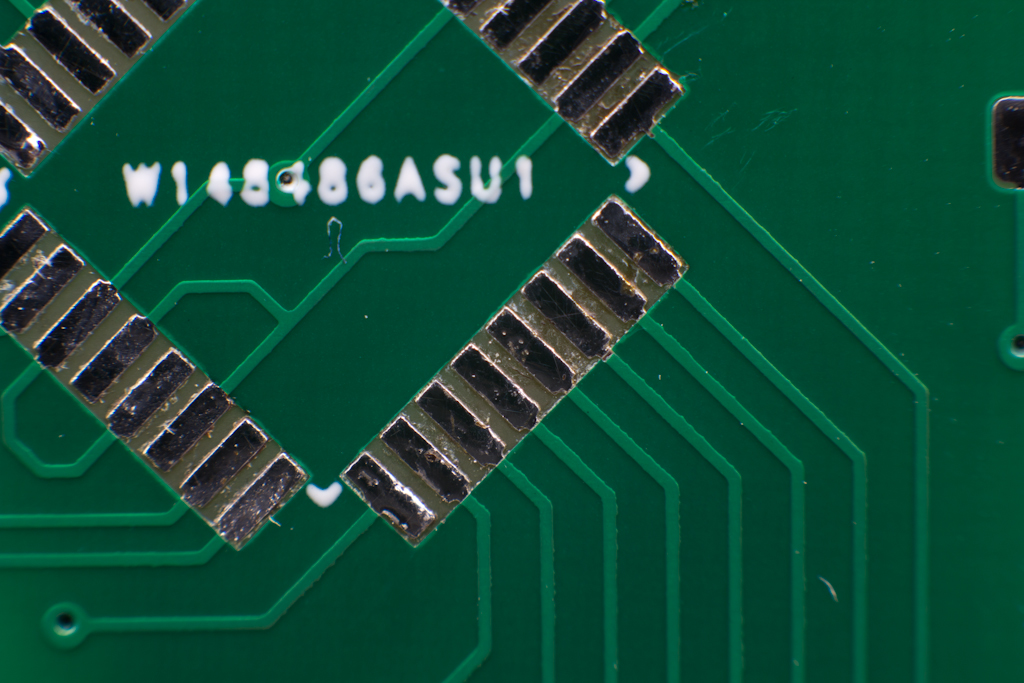
The board edges were milled cleanly. The internal slot was fabricated as per the design files and the drills for the mechanical holes, vias and plated through holes looked generally well aligned.
The initial visual inspection showed excellent consistency across all 10 copies of the test coupon. The solder mask looked uniform and the HASL surface finish was very smooth. There was a small, but definitely noticeable, amount of milled FR4 dust present on all the boards that had to be wiped clean; all the boards could have used a good blast with compressed air at the factory.
PCB Dimensions
All of the milled and drilled dimensions measured well within tolerance. For the board edge dimensions, the greatest variance from largest to smallest measured dimension in either x or y was 0.1mm. Board thicknesses varied from 0.01mm over to 0.07mm under, again, all within tolerance. The internal slot around the heatsink measured to within 10% of the 1mm expected width.
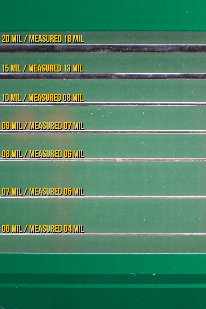
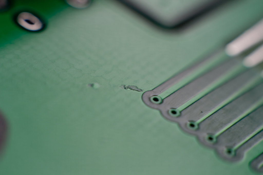
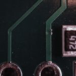
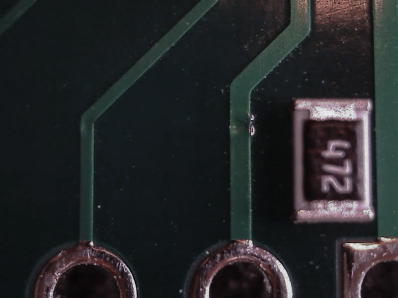
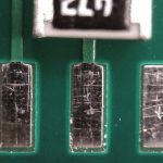
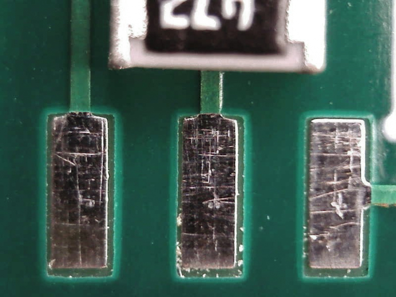
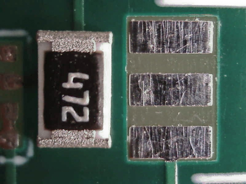
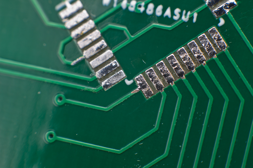
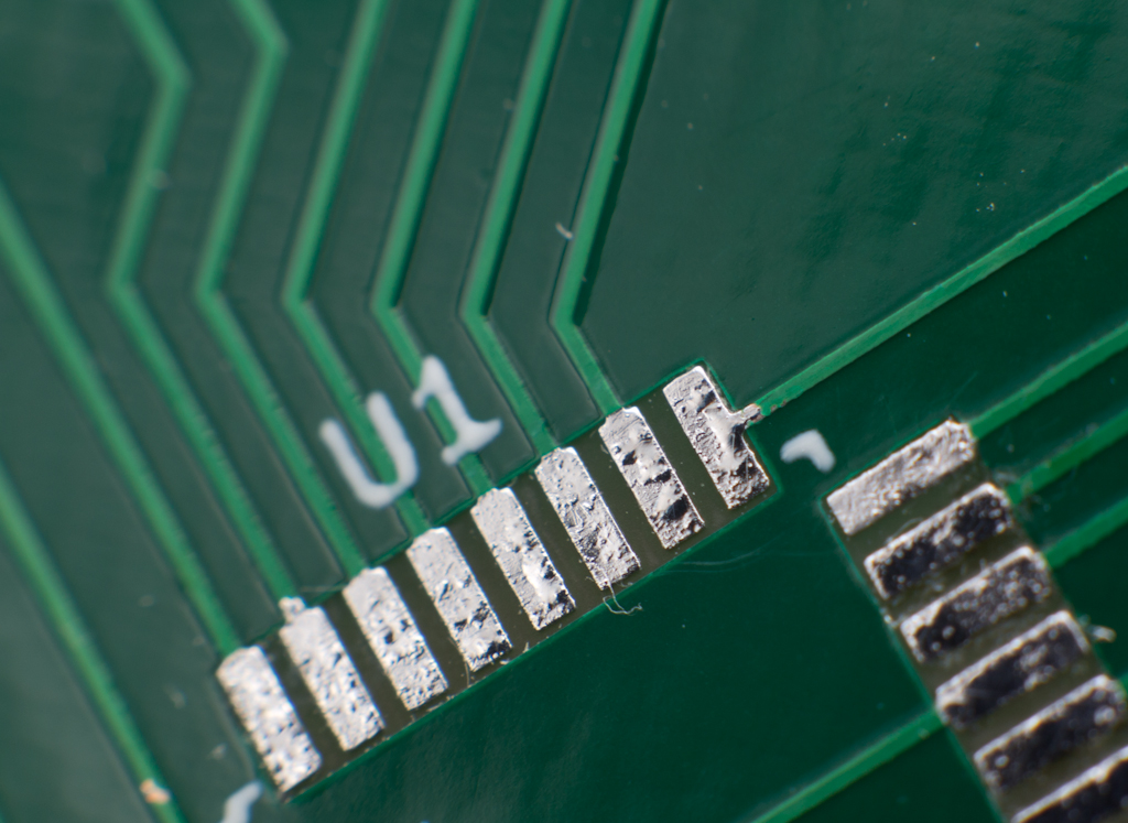
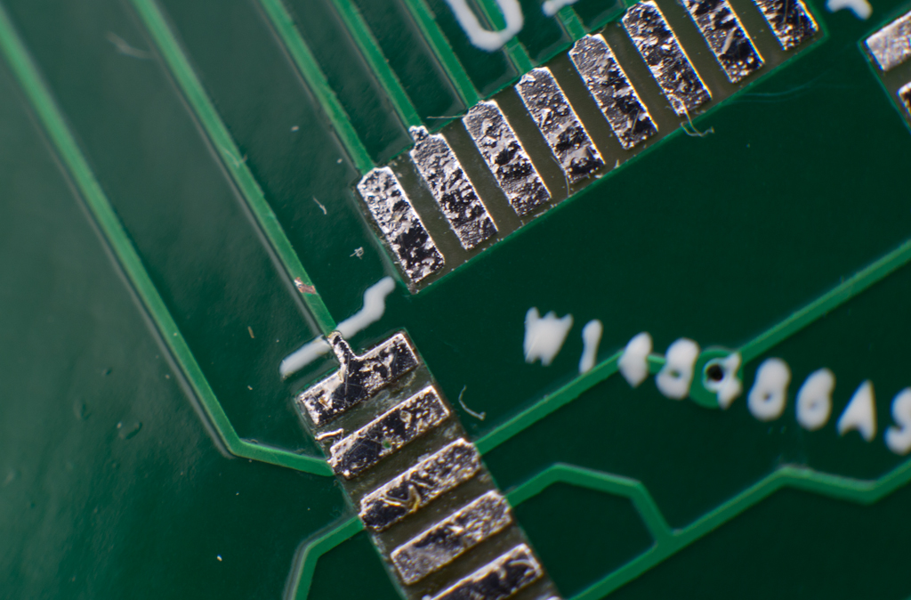
Unfortunately, the trace widths were universally smaller. All traces measured at least 2 mil undersized and on some boards were 3 mil under, cutting the 6 mil trace width in half. All 9 mil and narrower traces failed on all boards, and those showing 3 mil narrower traces all traces 10 mil and smaller failed as well. Additionally, this resulted in smaller footprints when measured in the heat sink area (off in both x / y by 2 or 3 mil depending on the board) and the copper thickness test area (off in width by 2 or 3 mil, length not tested).
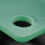
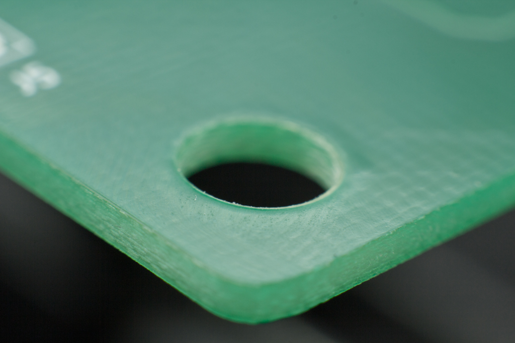
The M5 clearance holes passed for both size and location and were left unplated as per the design files. No burr was present around the large drills and the interior of the hole was clean cut FR4 exhibiting no burning or scarring.
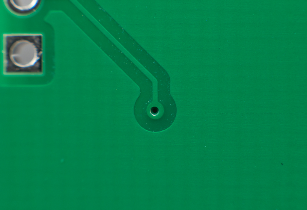
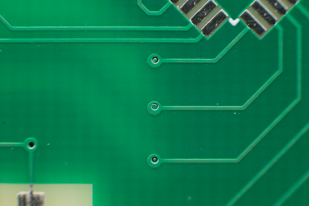
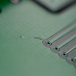
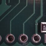
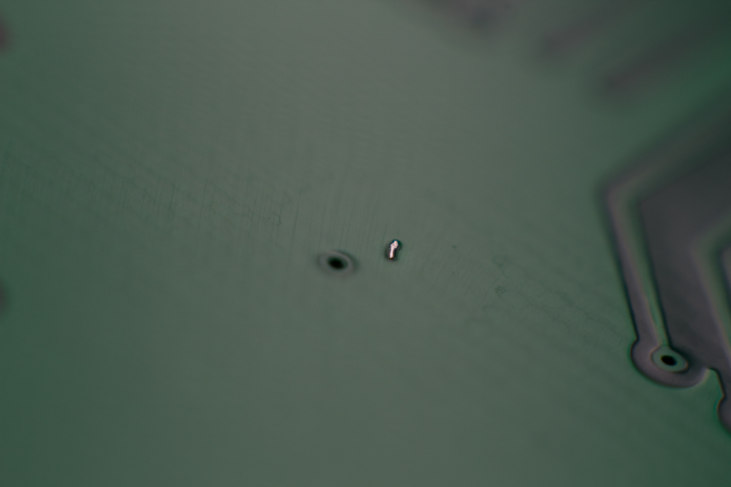
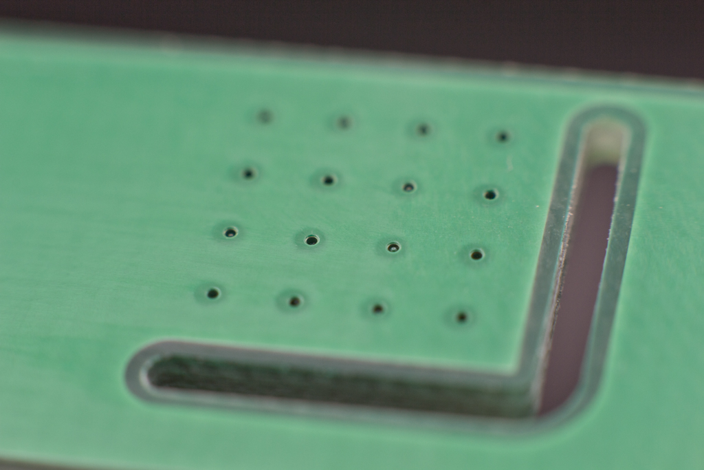
There were some via drill offsets but only one drill on one board approached the edge of the actual annular ring. The rest were either directly on center, visually, or only slightly off.
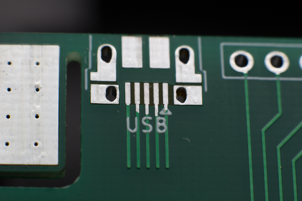
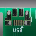
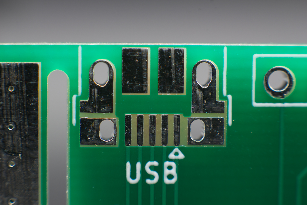
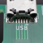
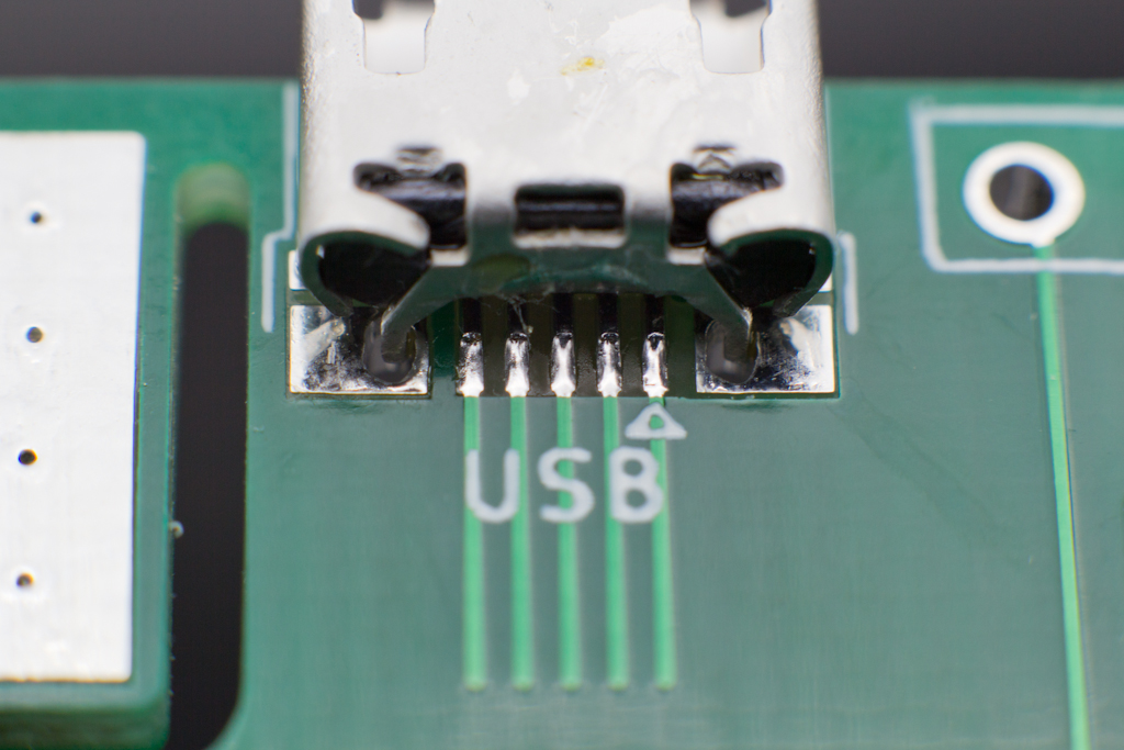
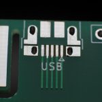
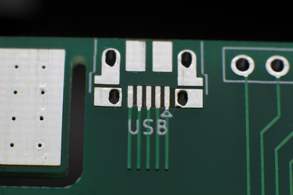
The milled and plated slots for the USB connector all showed either very exact or close to exact perpendicularity to the board edge.
PCBWay Test Report for 2019
-
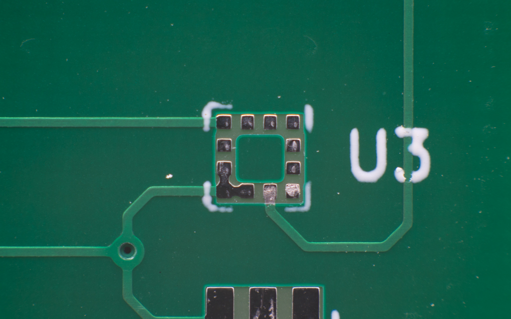
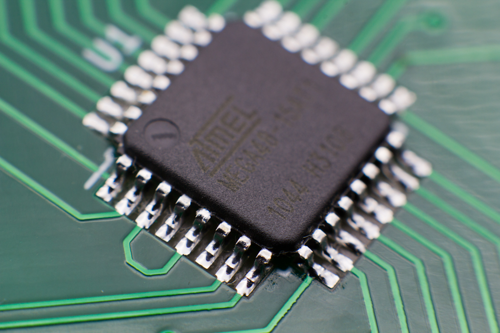
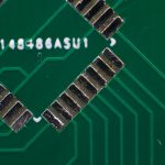
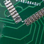
- Excellent QFN Footprint
-
- Straight Plated Slots
-
- Clean NPTH
-
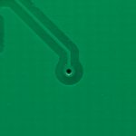
- Typical Via Drill Offset
-
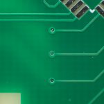
- Significant Via Drill Offset
-
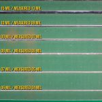
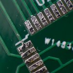
- Trace Widths Below Tolerance
Copper Layer Quality
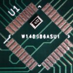
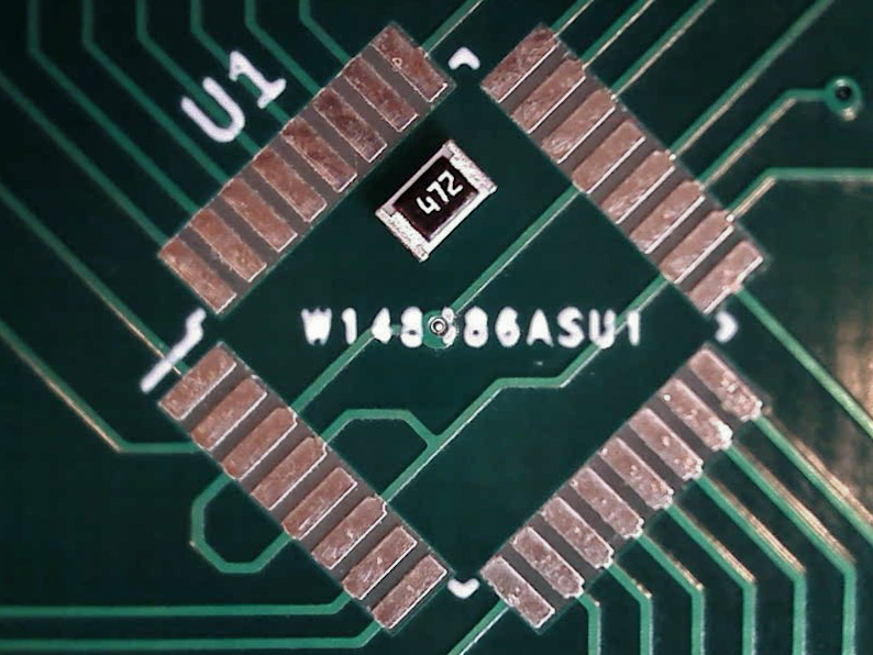
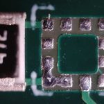
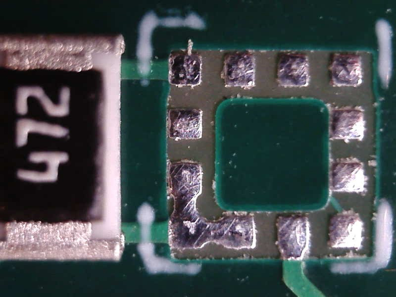
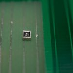
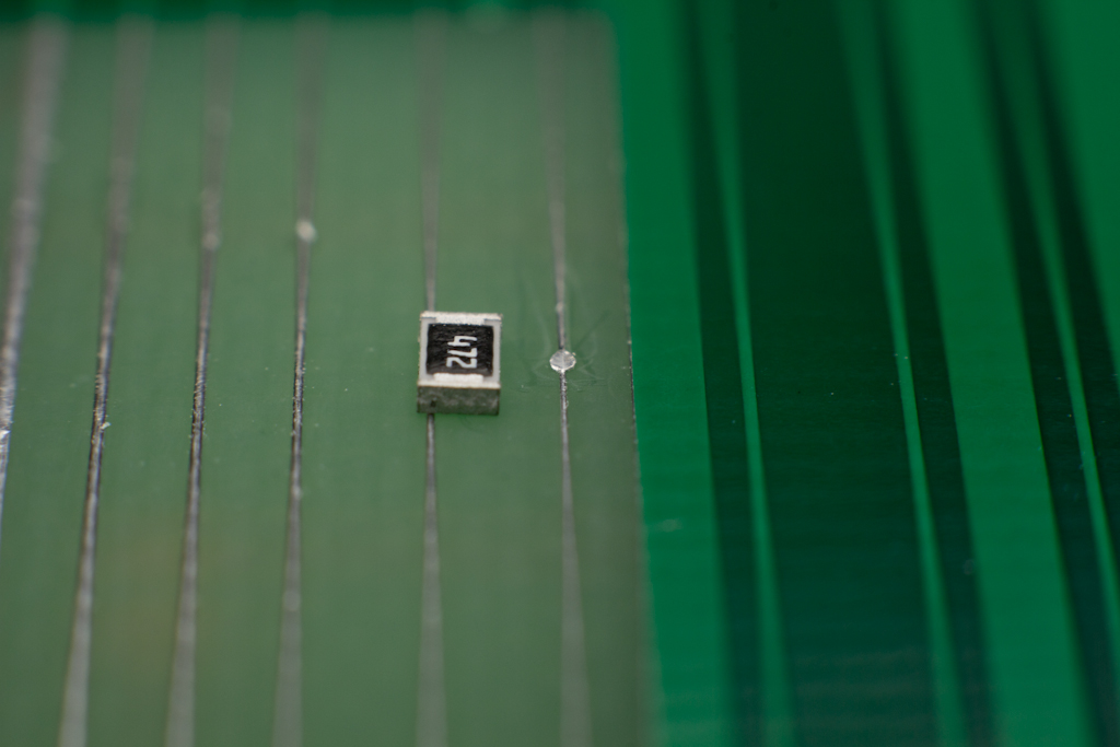
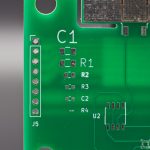
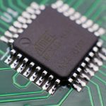
The QFN and QFP footprints were reproduced exceptionally well with clear pad definition around the QFN, even with the HASL surface finish. The passives footprints were of good quality and usable.
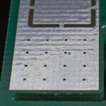
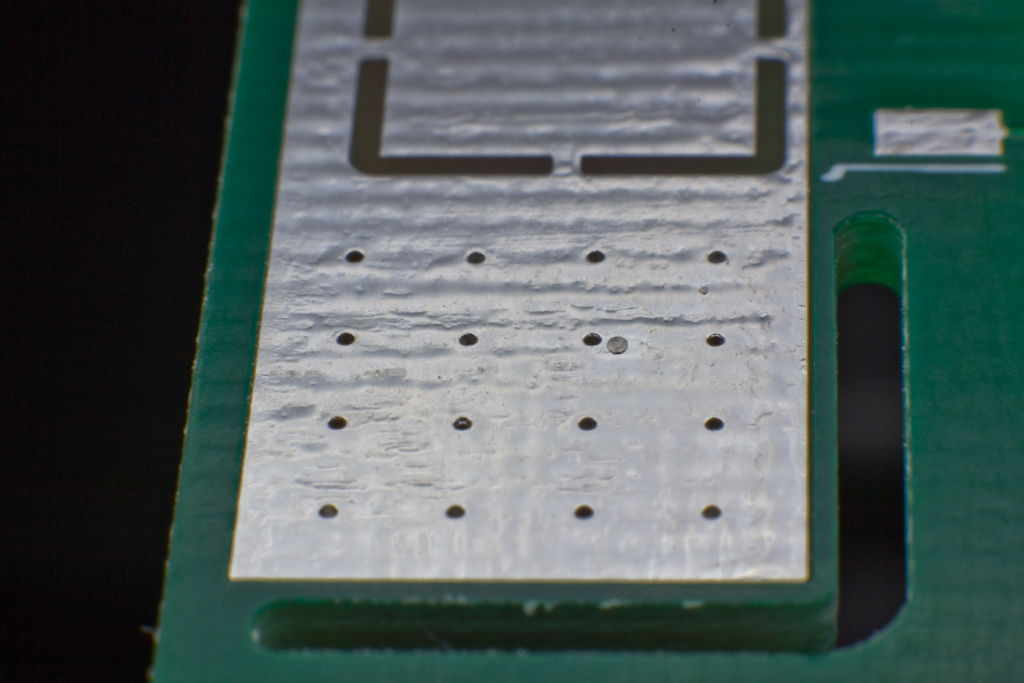
The HASL had a remarkably smooth surface finish, even on the smaller footprints where it can tend to turn into solder blobs, but on the PCBWay boards was very flat. Across the heat sink area it was evenly deposited with only slight surface variations.
All footprints were intact and the vias were undamaged.
Traces on two of the boards looked like they were slightly damaged prior to applying the solder mask, as though something had mashed into them slightly, and one of the exposed traces in the width testing area had a solder blob 11 mil in diameter pressed into it.
The backside copper ground pour was damaged on one board as well.
-
- QFP Footprint
-
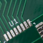
- QFN Footprint
-
- Solder Blob in HASL
-
- Damaged Ground Pour
-
- Solder Blob on Trace
-
- Damaged Trace 02

-
- Damaged Trace 01
Solder Mask Quality
The solder mask was uniform across all boards, with a visually even thickness. It extended edge to edge and the pad clearance was consistent across all boards. I was particularly happy to see consistency in the heat sink area on the back side mask. The only noticeable blemish was on a single board: a solder blob was melted into the mask.
-
- Solder Mask Clearance SOIC8
-
- Solder Mask Clearance SOT23-5
-
- Solder Melted into Solder Mask
-
- Quality Solder Mask Over Via Stitching
-
- Solder Mask Over Via Stitching
Silkscreen Quality
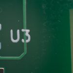
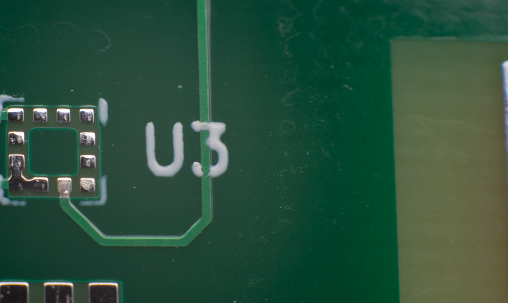
The PCBWay silk screen appears to be done with a low cost print method rather than photo quality screening, but as these boards cost around 0.50 USD a piece, that’s to be expected. Quality was good across all the boards with the only exception being where the print crossed a trace, occasionally resulting in a disrupted character.
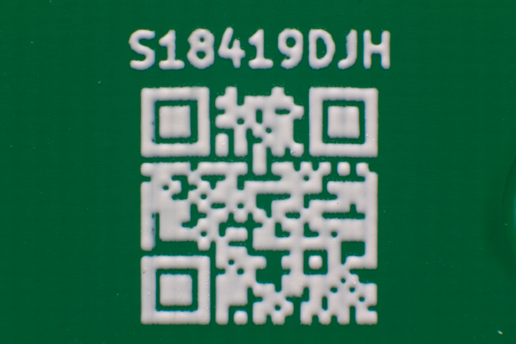
The quality of text in the passives area was well represented across all text sizes, all of which were easily readable even without magnification. However, resolution was insufficient to crisply reproduce the 1cm QR Code, which is too fuzzy to scan correctly without magnification.
PCBWay did print a manufacturers mark on the board, but in deference to how much their customers hate those things, they did place it right where the QFP would go so a soldered board would hide it. I found that to be a nice touch. Of course, I could have paid the $3.00 to prevent having the mark in the first place.
-
- Crisp Passive References in Silk Layer
-
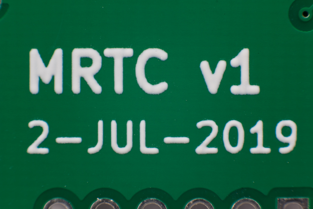
- Board Name
-
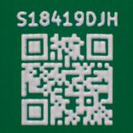
- QR Code Resolution
-
- Silkscreen Over Trace Issue
-
- Manufacturers Mark
Solderability
A random board was selected and the soldering tests were run through. Both the Micro USB Connector and the QFP32 sat flush against their footprints, and soldered down easily. I found the QFP32 very easy to move into alignment while tacking down a corner pin.
The solder mask around the QFP showed increasing erosion after each cycle of rework. The mask began deteriorating from the pads back up the traces and in a few instances, also degraded in areas close to , but not connected to the pad or any other areas of erosion. No pads lifted while pulling the part up during rework.
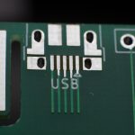
The USB Connector showed little mask degradation after the first rework, however the erosion continued along the solder resist covering the traces leading from the connector after the second rework.
The silk layer didn’t discolor from the heat or the isopropynol.
-
- QFP32 Initial Soldering
-
- Micro USB Initial Soldering
-
- QFP32 Pads After First Rework
-
- Solder Mask Erosion After Second Rework
-
- QFP32 After Second Rework
-
- Continued Trace Erosion Post-rework
-
- USB Connector After First Rework
-
- USB Connector After Second Rework