


DirtyPCB PCB Review

Dirty PCBs
US Based Order Aggregator / China Based Manufacturer
$1.70
10
10
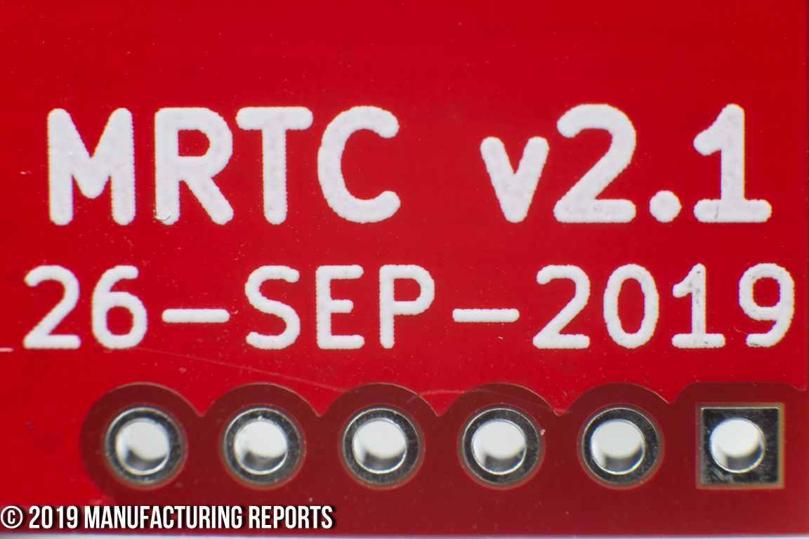
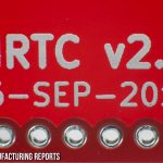
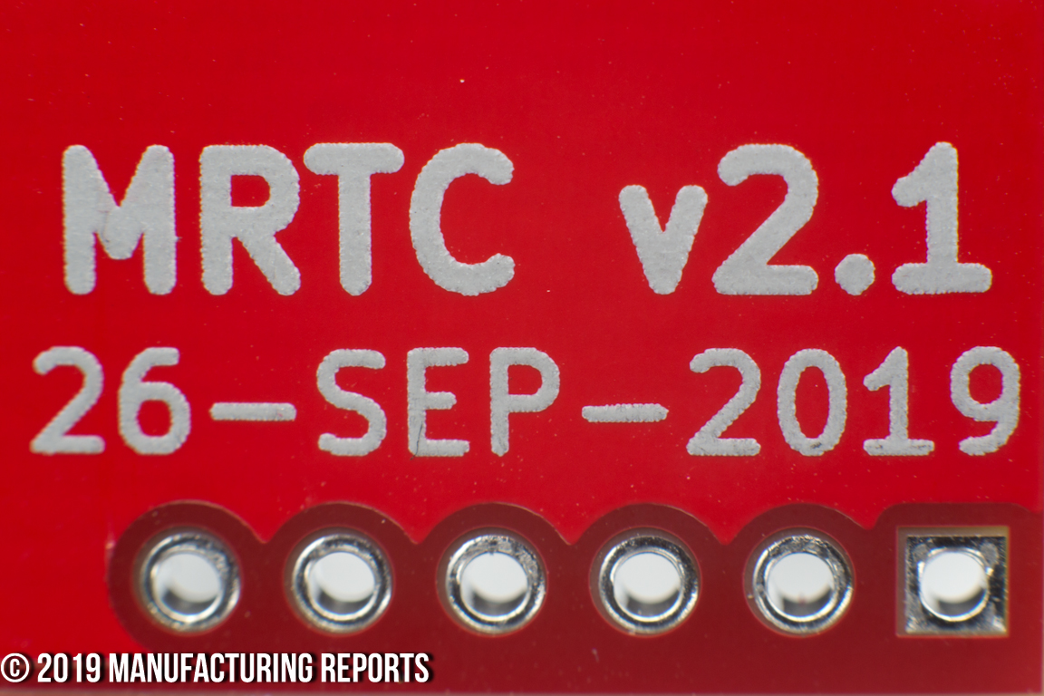
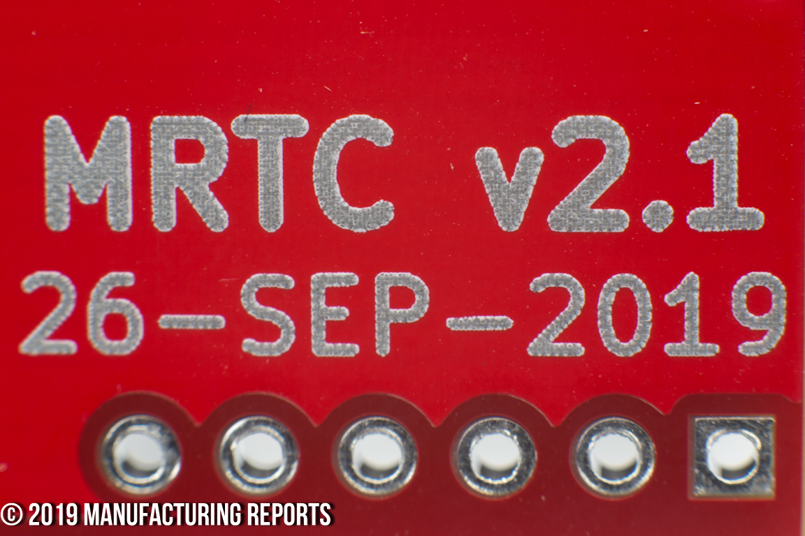
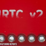
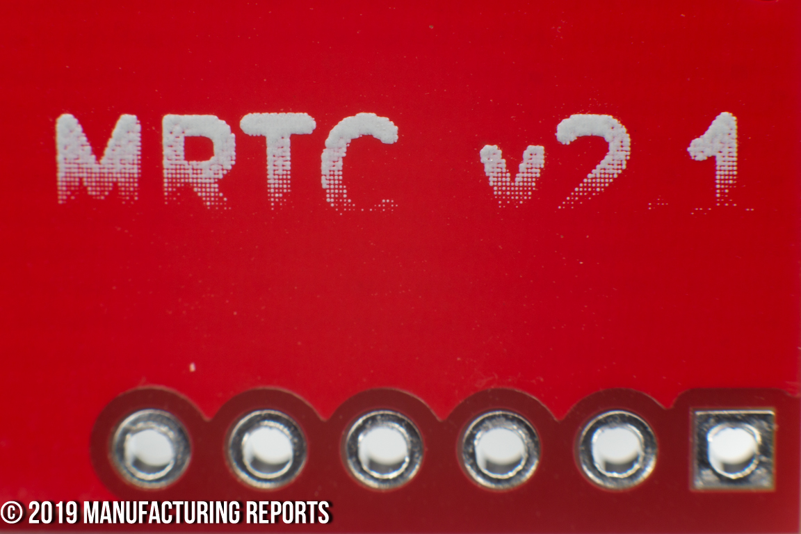
MRTC v2.1
Upfront About Quality
Easy to Find Design Rules
Shipped on Time
True LPI Silkscreen Process
Take It or Leave It Attitude
Limited Stackup Options
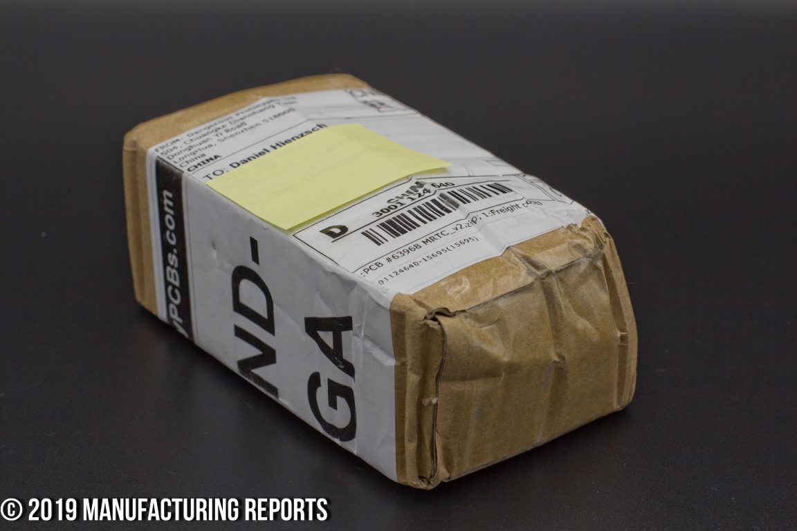
Poor Order Packaging
No Adherence to Dimensional Tolerance
Boards are Absolutely Filthy
Mechanicals Were Incorrectly Plated
Contaminant Everywhere
Beautiful Silkscreen Badly Applied
DirtyPCB has been around for quite a while now, and I gave them a couple of protopack orders way back in 2015. They are a part of Where Labs, LLC and therefore a subsidiary (partner? distant relation?) of Dangerous Prototypes. The DirtyPCB site has developed extensively since then with various manufacturing offers from laser cutting to SLA 3D prints, BOM management and, of course, PCBs.
DirtyPCB really goes out of their way to set your expectations as a customer: you should expect fully functional boards, but not exquisite quality, although sometimes exquisite quality might slip through.
Cost
Final cost for a 10 board “Protopack” in the 10cm x 10cm dimension range from DirtyPCB was $16.95 with an additional $21.00 in DHL shipping from whoever is making their boards in Shenzhen. That boils down to $1.70 per board.
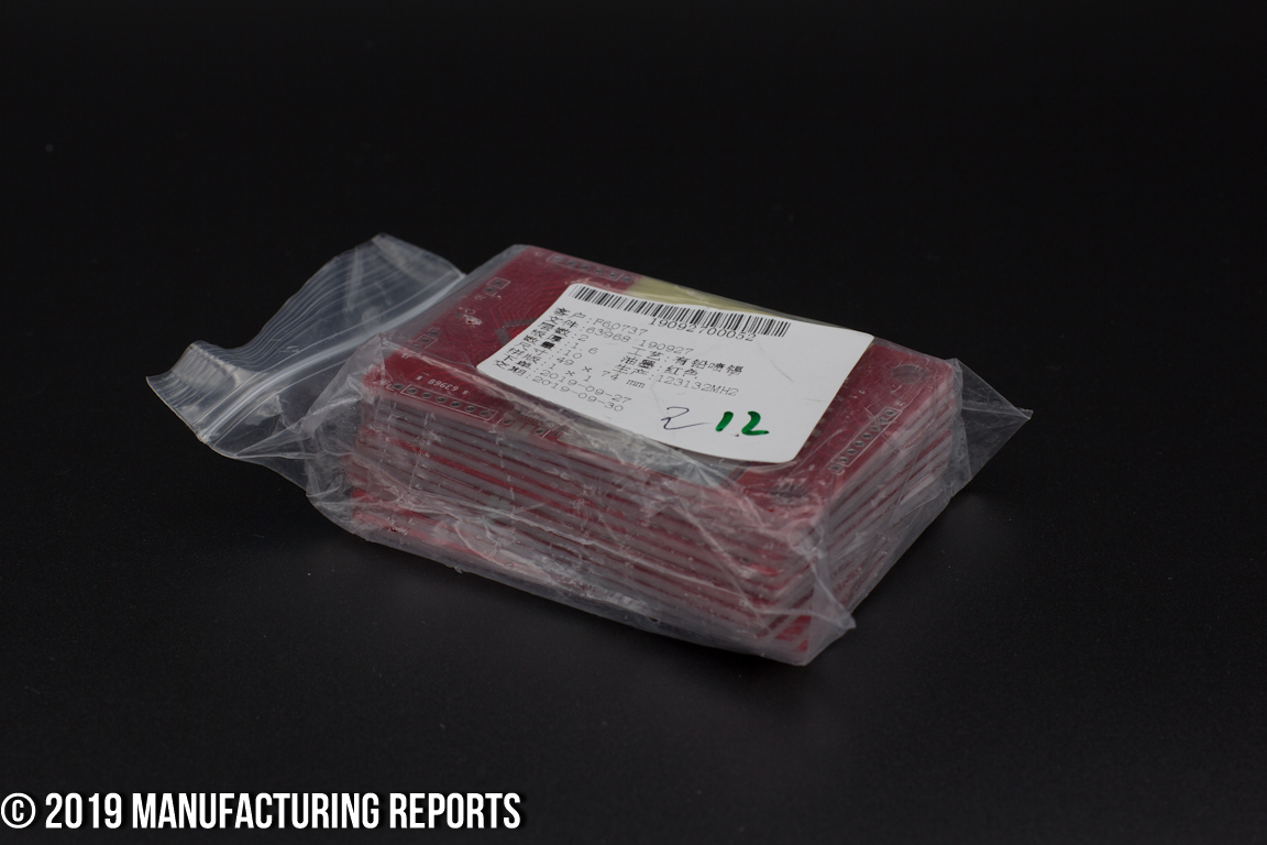
Ordering the Protopack is a bit of a gamble, as the quantity you’re ordering is “±10”. You’ll probably get more than ten, maybe as many as 12 boards, but you may also get less. I imagine it depends on how their nesting algorithm builds out the panel. In this case I received 12.
Ordering
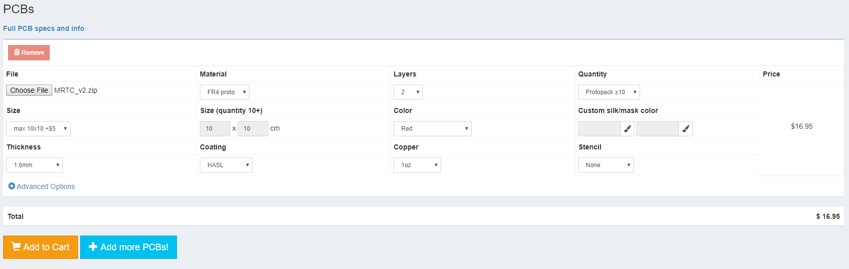
Getting to the order page is pretty simple, as it’s the default page when you go to the DirtyPCB URL. The zip file of Gerbers was selected and the specs laid in for the limited stackup options available. There is an advanced options selection area where you can select Vgroove board separation, where you want the order markings (top or bottom layer silk), and turn time, all of which I selected as defaults.
Because the amount of ordering options are limited, and because care was taken to make sure the ordering process was exceptionally streamlined, I was able to slide straight through the ordering process from gerber selection to payment processing in just a few minutes, and an order confirmation was received moments later.
-
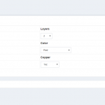
- Ordering Options
-
- Order Status
Fulfillment
The boards arrived in a DHL pack, with a ratty, beatup, cardboard box inside. That had a ziplock bag of 12 boards in it, crumpled up in bubblewrap. The boards weren’t vacuum sealed or rubber-banded together so they were free to abrade against each other a bit during shipping.
-
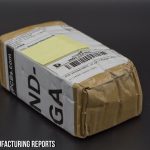
- Order Packaging
-
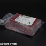
- Board Packaging
Customer Service
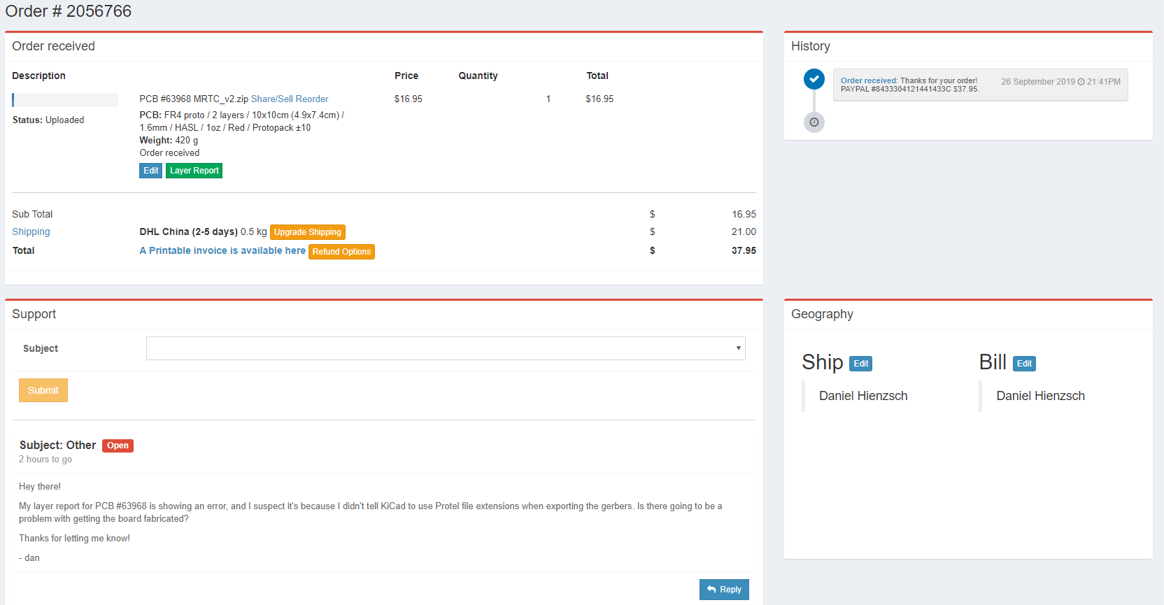
The order status page is very easy to read, with everything boiled down to a single page. A layer report is available, and sure enough, there was an error reported on the outline, because all the gerber files had the same .gbr file extension instead of Protel extensions. A support request form is built right into your order status page, making it easy to ask a question right away, so that’s what I did, generating a support ticket available to view on the status page, as well as an email to track it with. A few hours later, I received a note saying they had reviewed the gerbers and no issues existed.
Design rules are easy to find, beneath the “Full PCB specs and info” link right on the order page, which also clearly states what sort of service and quality you should expect.
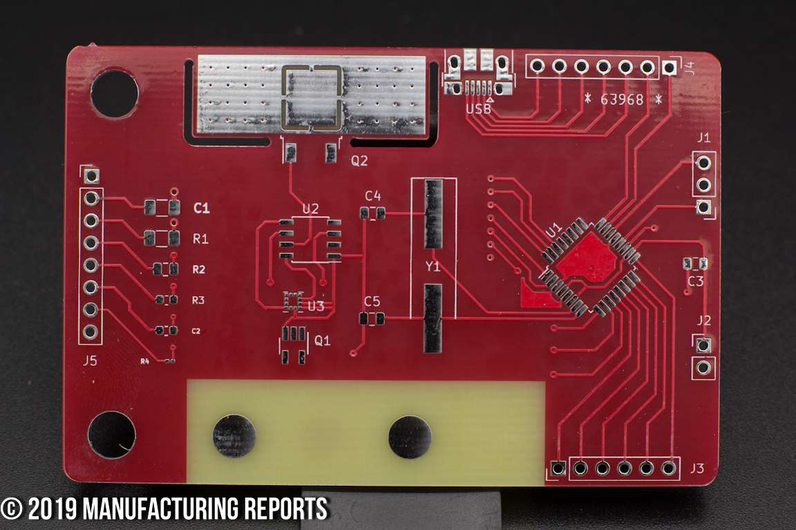
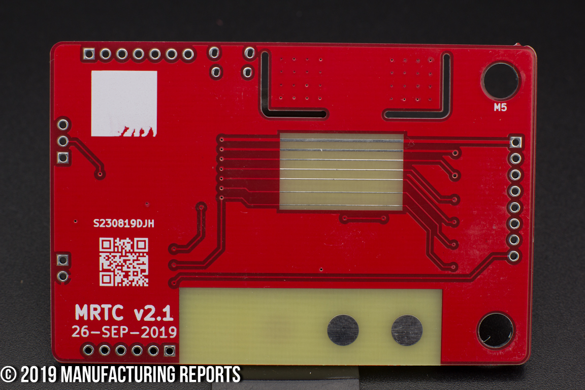
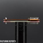
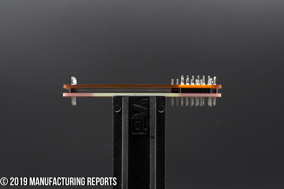
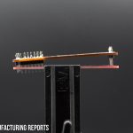
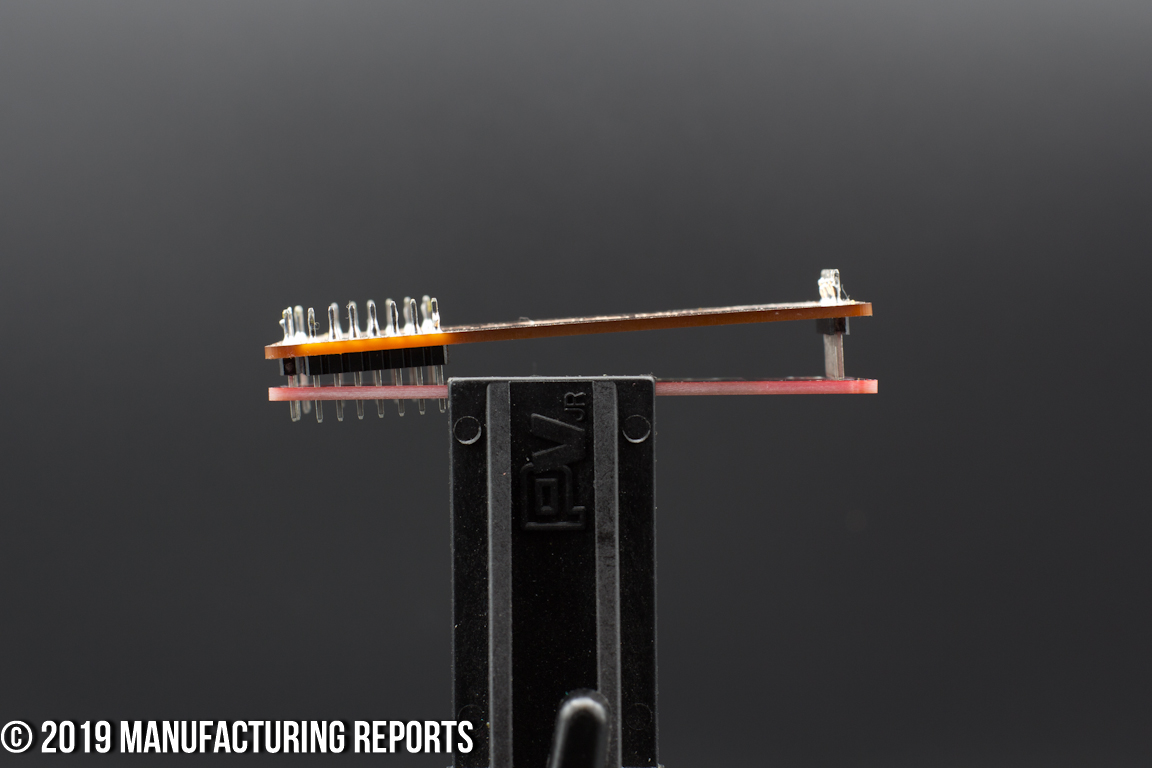
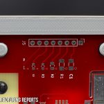
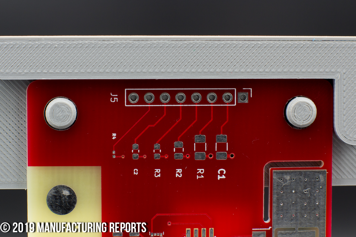
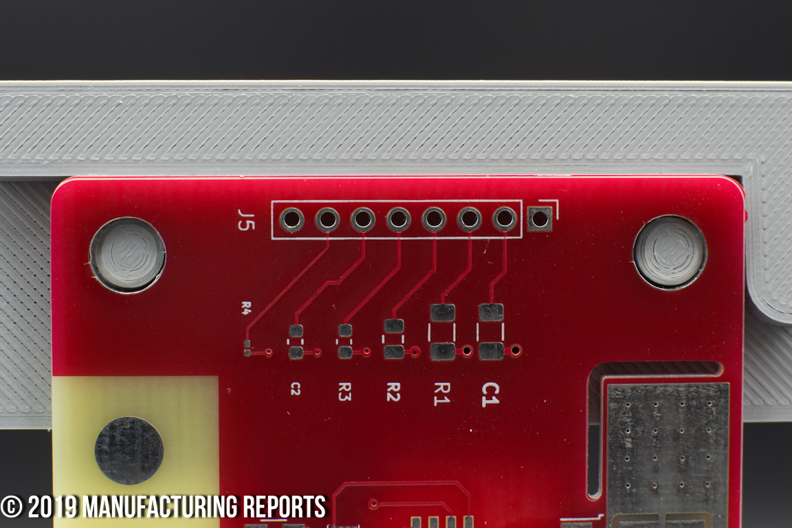
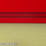
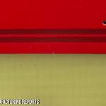
Circuit Board Visual Inspection
-
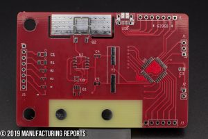
- Dirty PCB Review Full Board Front
-

- Dirty PCB Review Full Board Back
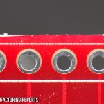
Even taking into account the low expectations that Dirty PCB attempts to set on their “About” page, these boards were subpar.
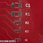
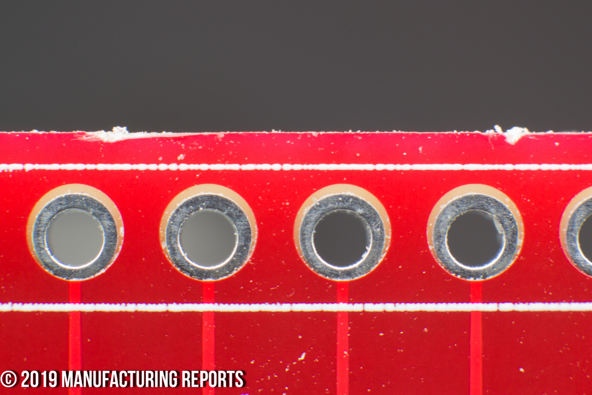
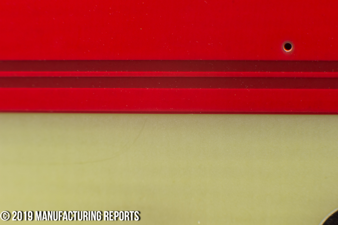
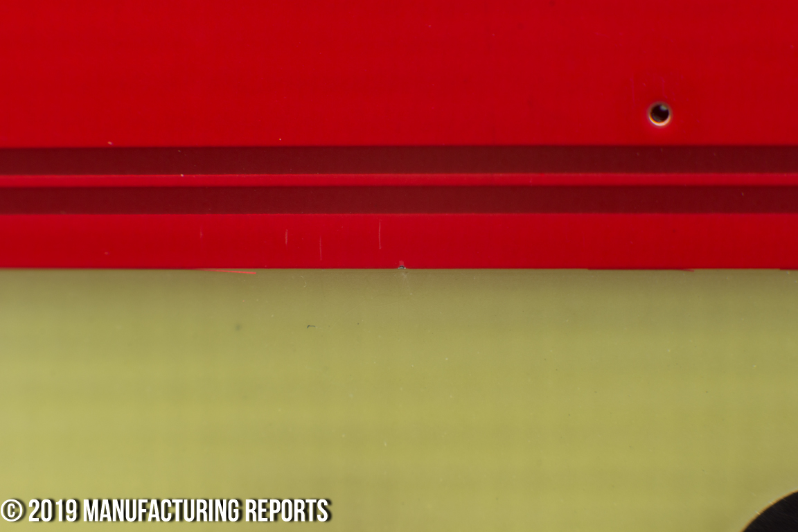
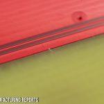
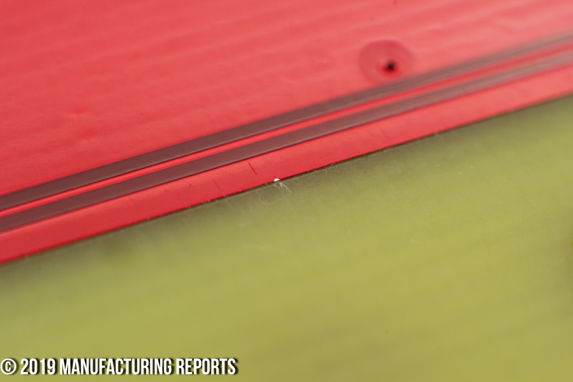
They were absolutely coated in milling dust. Okay, fine. Not only do they call themselves, “Dirty PCB”, but I don’t score for “board is dusty”. Unfortunately, I see a pattern between dust on PCBs and poor dimensional tolerance and these boards failed dimension tests left and right, showing a lack of even basic precision in the milled features.
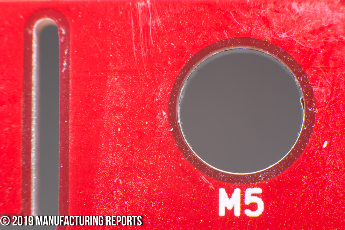
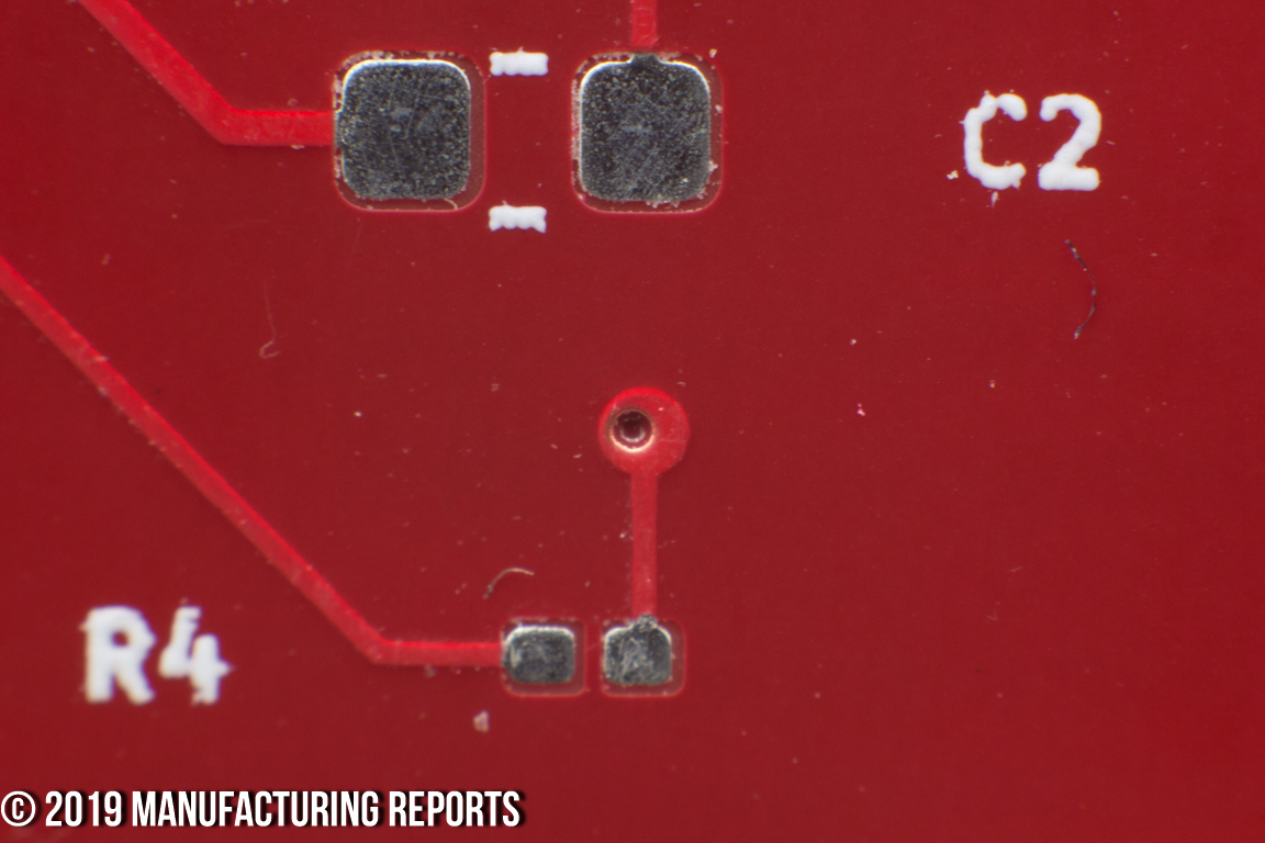
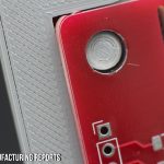
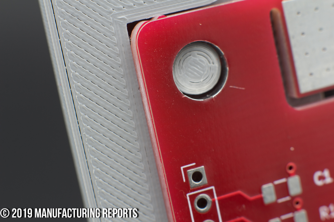
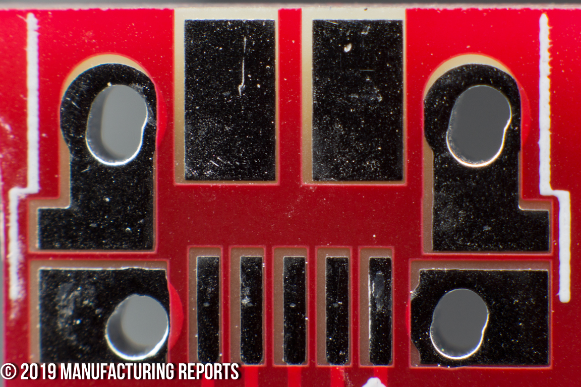
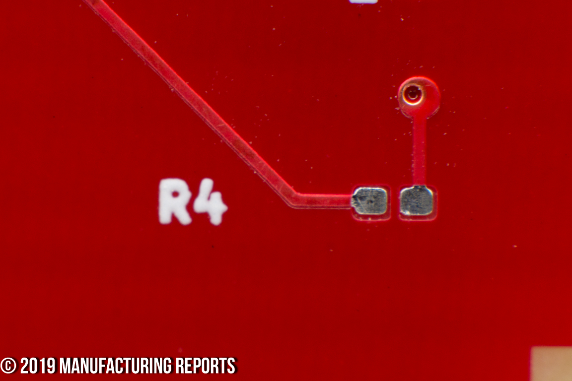
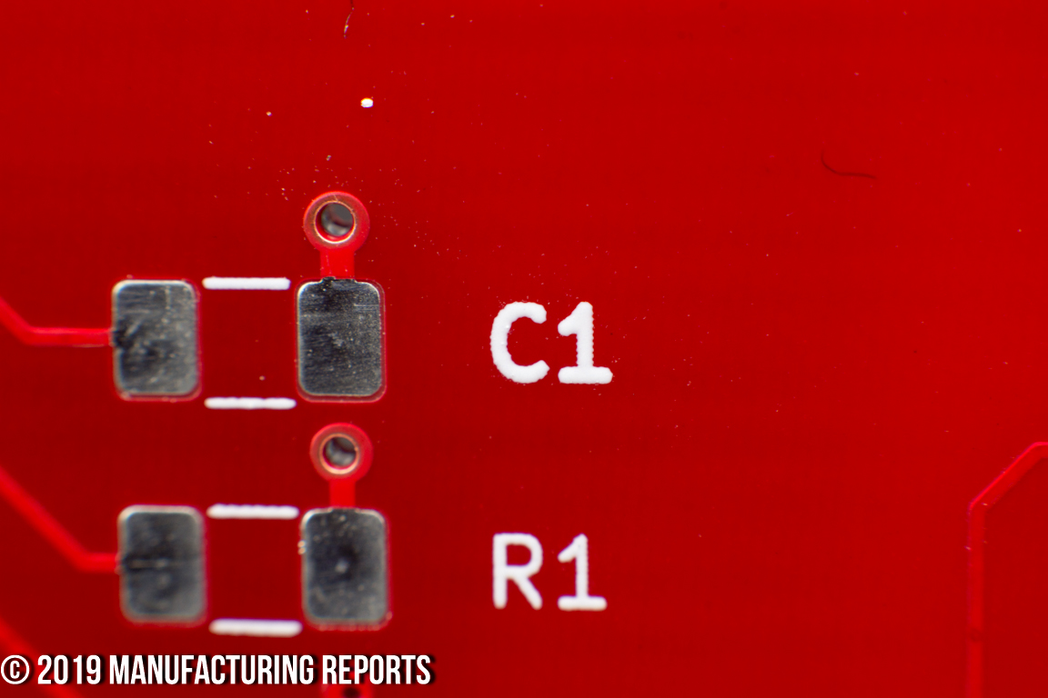
Every board had issues with contaminant and in one case a chunk of stuff under the solder mask was so big, I thought it was a tented via at first. The mechanical holes were not supposed to be plated, but did receive it and received it poorly. On many boards the plating has delaminated , and hairs of FR-4 and plating were trapped under the mask layer.
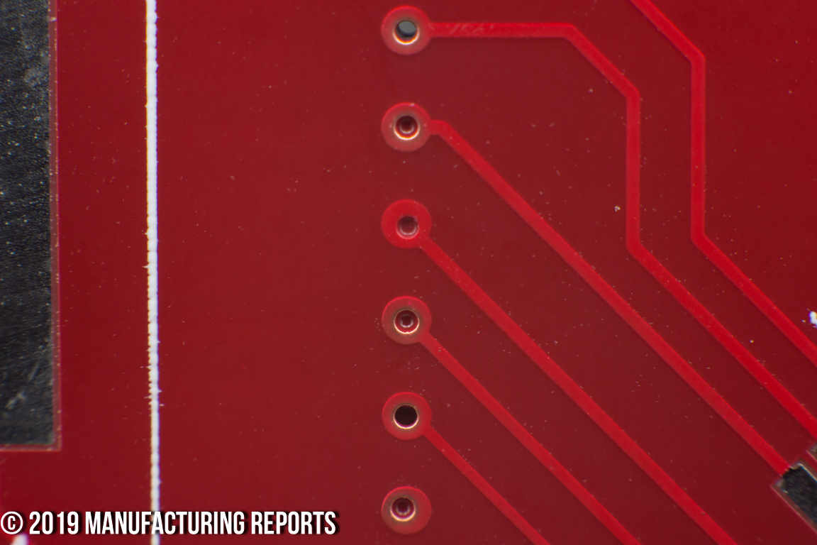
The via drills were all over the place and nearly intersected the edge of the annular ring in several locations. The plated slots are the worst I’ve seen, being offset from perpendicular at least 15° on all boards and by 45° on one, as well as being clogged with HASL to the point of not even being slots anymore, potato shaped or otherwise.
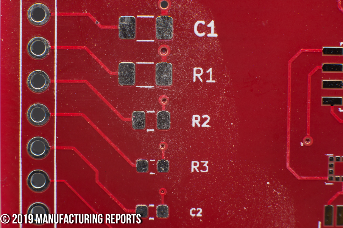
I want to praise the quality of the silk layer, since it is created with an actual liquid photo-imageable process and not DLP, and shows a crisp resolution down to even the 0.5mm font size. Unfortunately, either the screen was clogged or the system ran out of ink leaving whole areas of several boards with misprints or no print at all.
-
- Crud on Pads
-
- Dust on Board Backside
-
- Dust Close Up
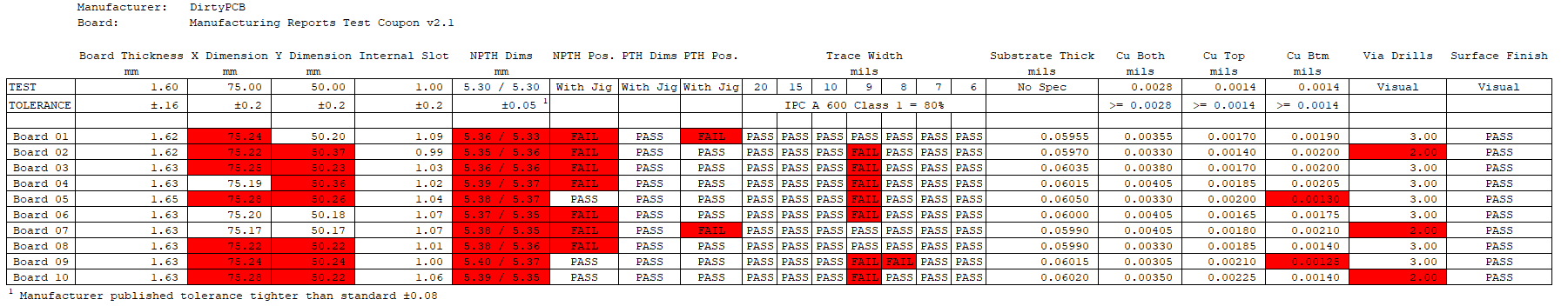
PCB Dimensions
These boards were a tolerance nightmare.
- Outer Dimension Within Tolerance: 2 boards out of 10
- Trace Widths Within Tolerance: 3 / 10
- NPTH Milled Feature Within Tolerance: 0 / 10
- NPTH Position Within Tolerance: 3 / 10
- PTH Position Within Tolerance: 8 / 10
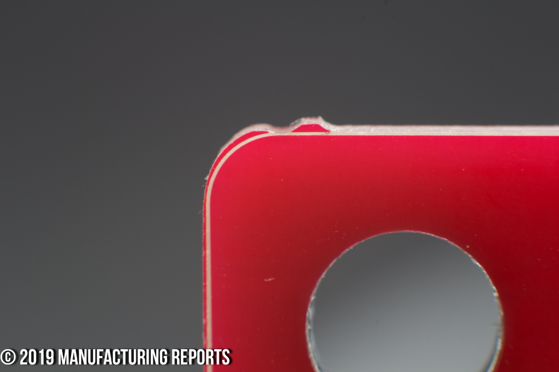
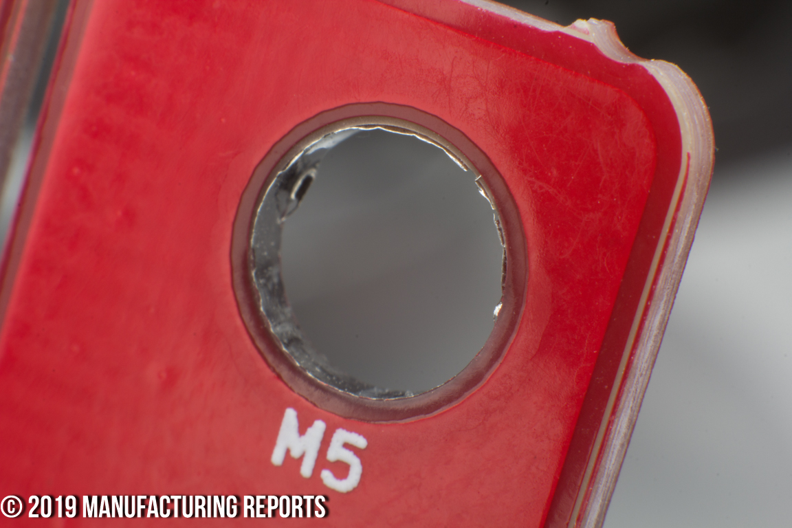
Beyond that, several boards had areas where the milling process gouged or delaminated the substrate and solder mask. The “NPTH” or “Non Plated Through Holes” did actually become plated, and plated very badly. There were chunks on the edge of the board from the edge cut that threw the dimensions way out of bounds. The plated slots were so cock eyed that in some cases they’re actually 45 degrees from perpendicular to the board edge.
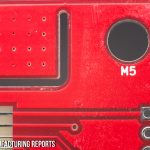
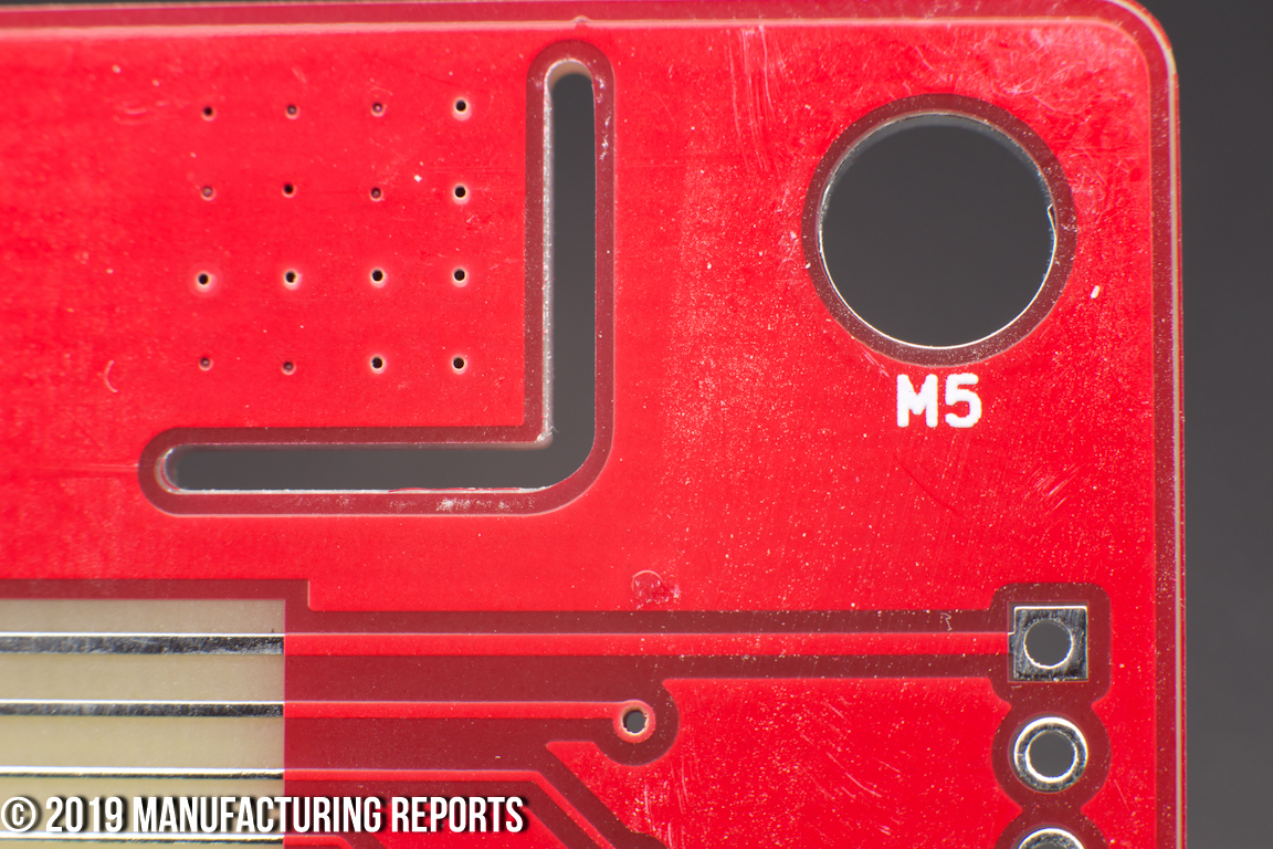
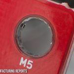
I was most shocked that several boards failed the plated through hole jig test. Essentially a daughter board is mated with the PCB, using the 0.1″ pin header positions around the outer edge of the board. Usually, I find this to be a relatively loose fit. With the Dirty PCB boards, two boards simply didn’t mate at all, the tips of the pins too far off center to slide into place without bending. For the boards that did fit, they were decidedly snug requiring careful positioning to mate successfully. The NPTH positioning was bad too, with three boards failing on all three mating edges near the M5 clearance holes.
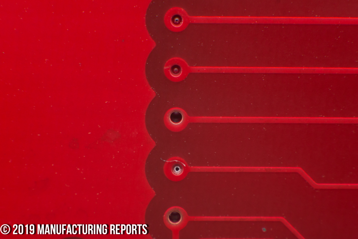
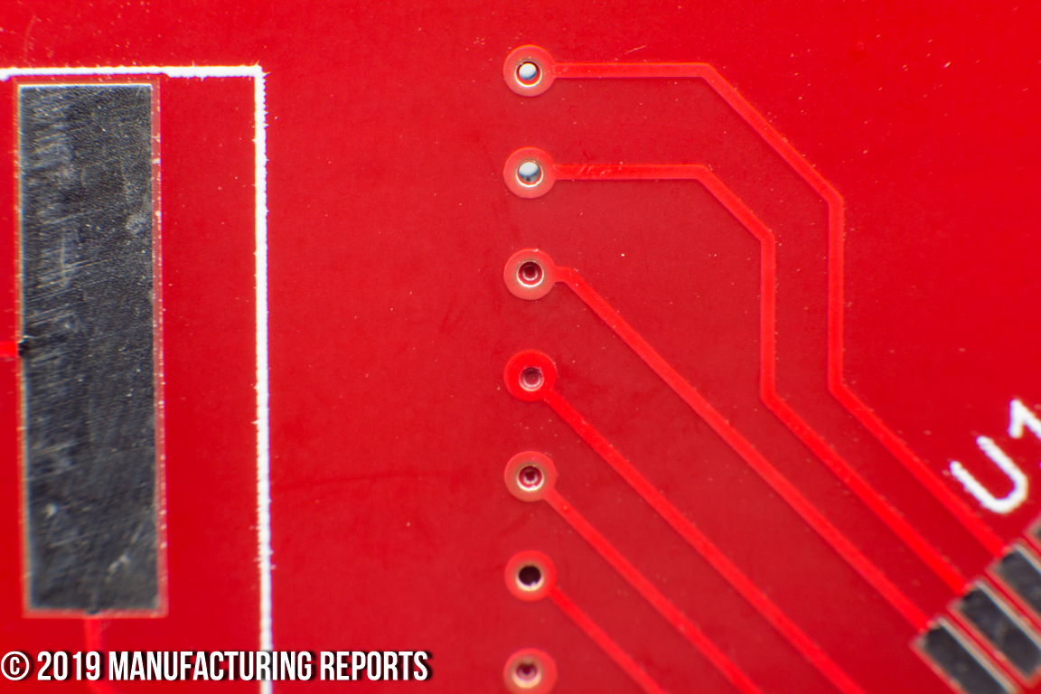
Via drills were all over the place, with every board having multiple points offset by the radius of the via drill size and in several cases, nearly intersecting the edges of the annular ring. Not bad enough to fail any of the boards, but very close.
Trace widths had a strange anomaly at the 9mil size.
Dirty PCB Test Report 2019
-
- Witness Mark Chunks
-
- Rough Edge Cut
-
- Rough Milled and Plated NPTH
-
- Strong Via Offset
-
- Random Via Offset
-
- Via Drill Offset
-
- Inconsistent Via Drill Size
-
- Poorly Milled Plated Slots
-
- Opposite Plated Slot Offset
-
- PTH Jig Pass
-
- PTH Jig Fail
-
- NPTH Jig Pass
-
- NPTH Jig Fail
-
- NPTH Jig Fail Detail
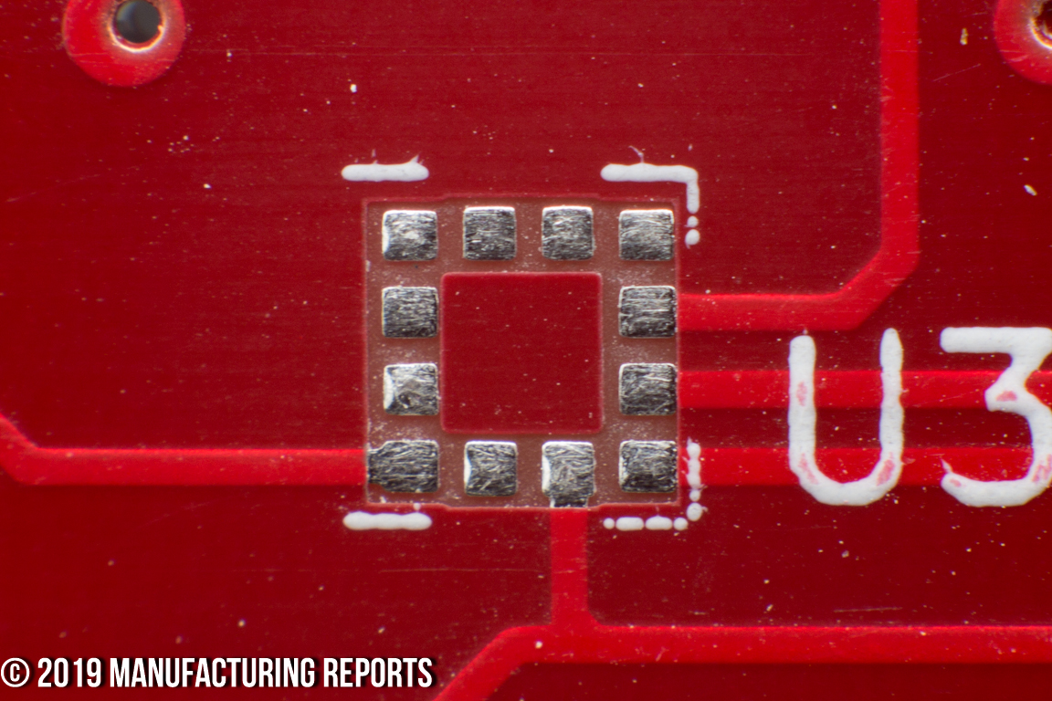
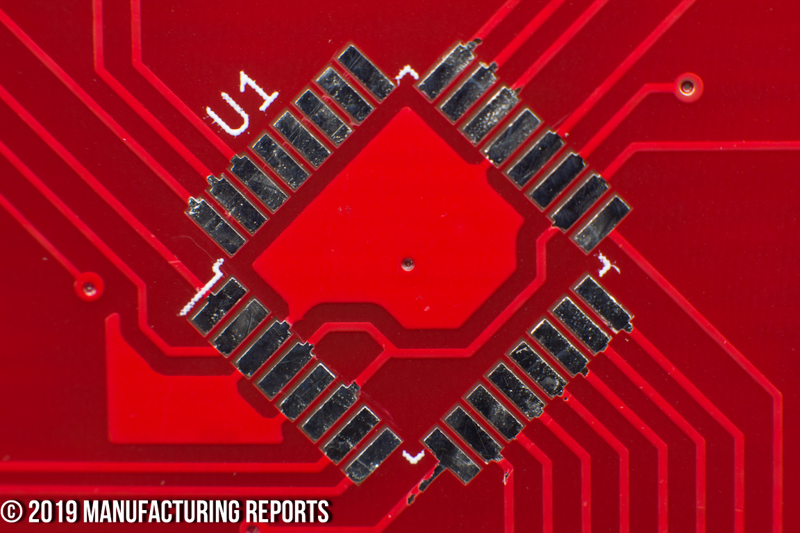
Copper Layer Quality
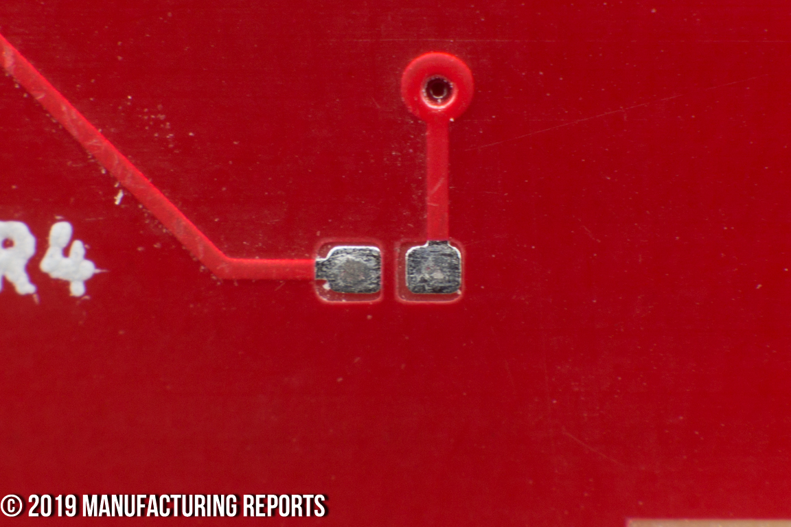
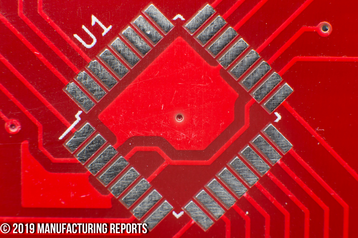
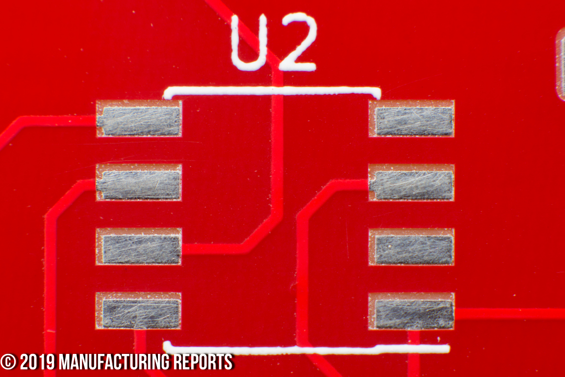
None of the traces or vias were damaged, and the half and sub-half millimeter footprints were all present and well formed. While two bottom side copper weights came in under tolerance, it was barely so by a handful of tenths of a mil, but under tolerance nonetheless.
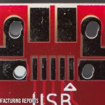
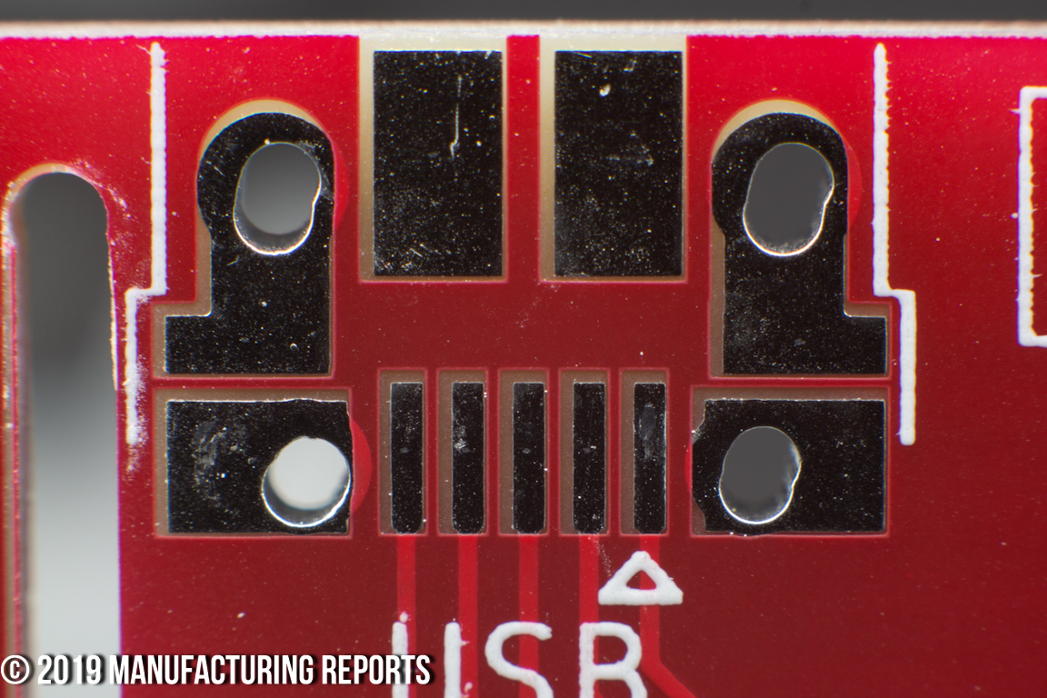
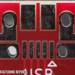
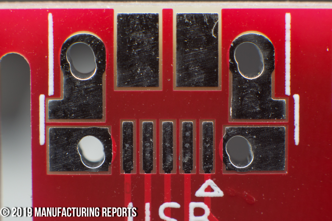
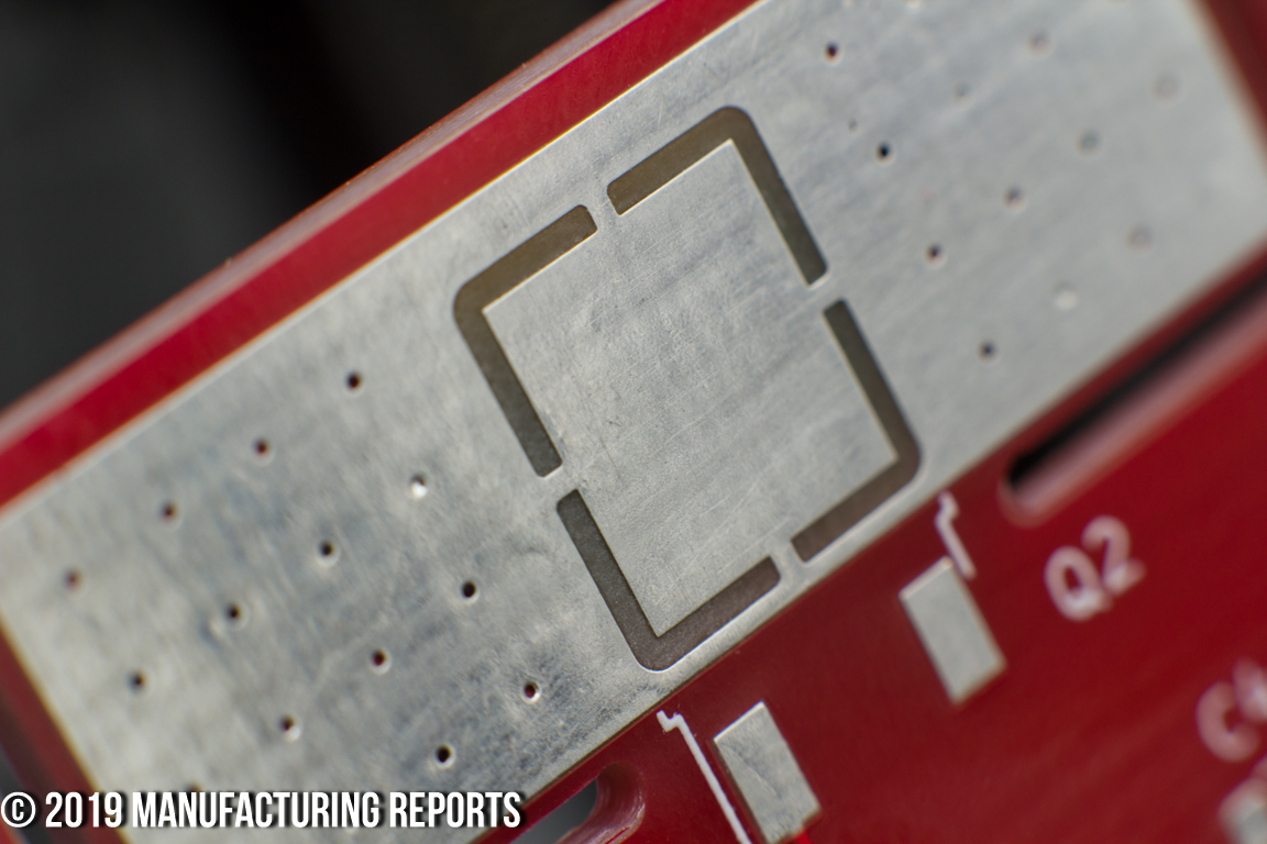
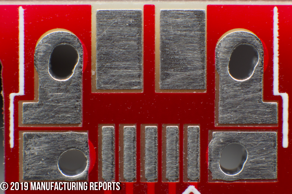
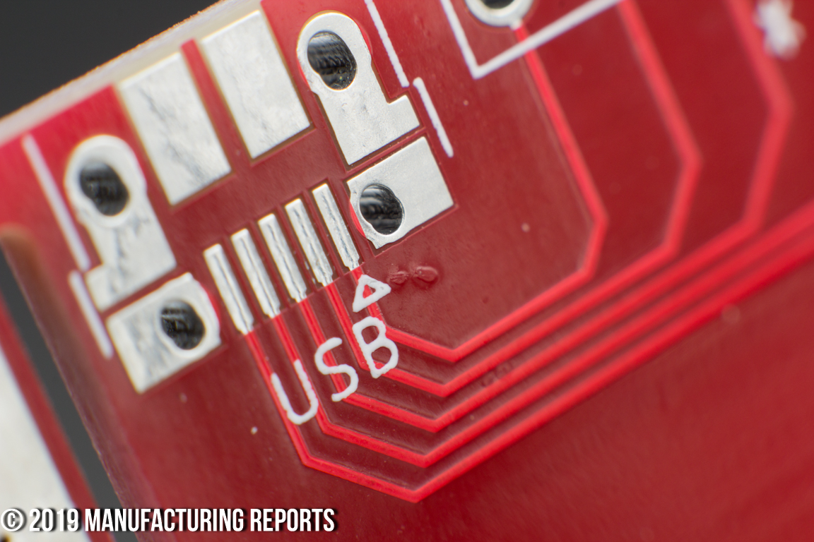
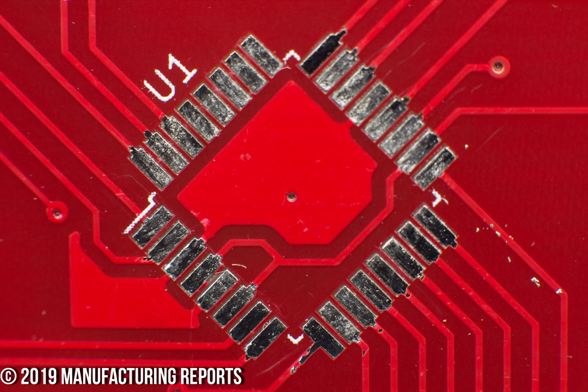
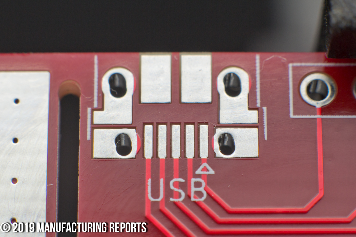
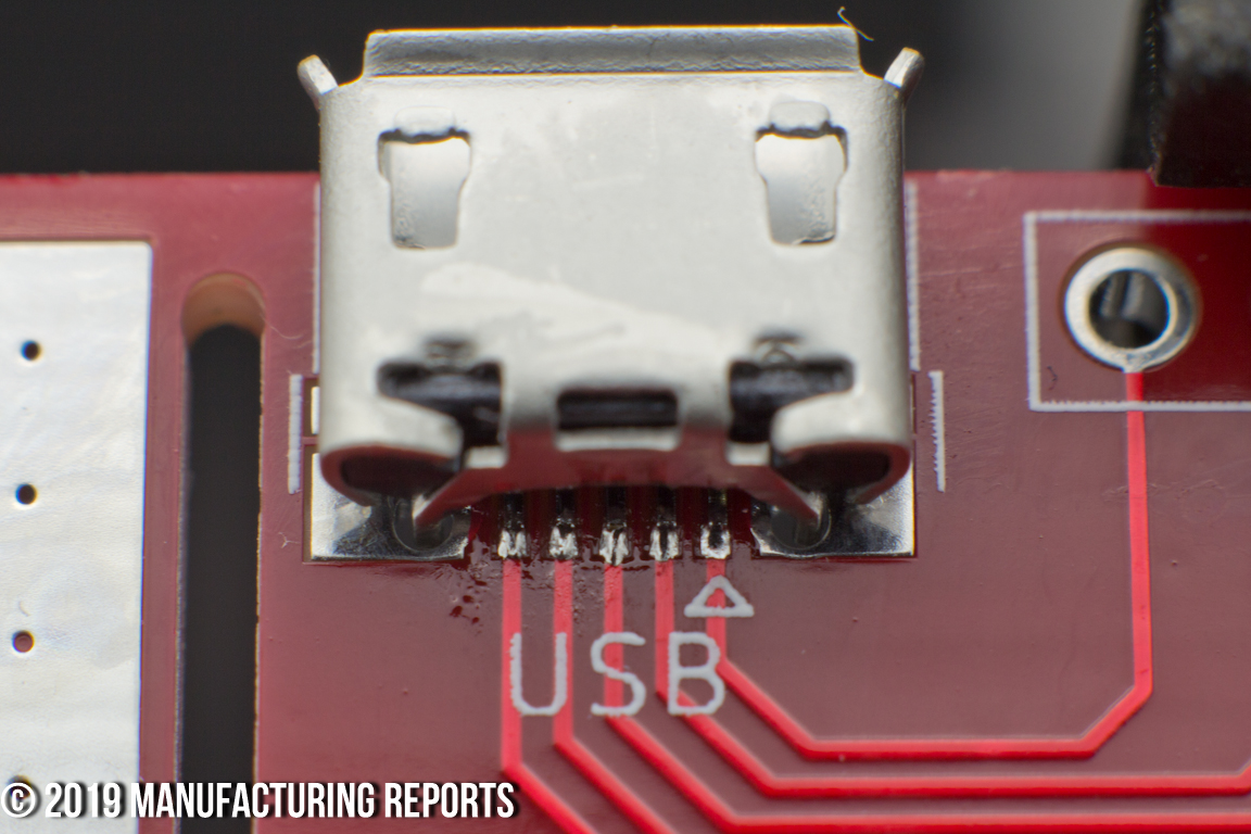
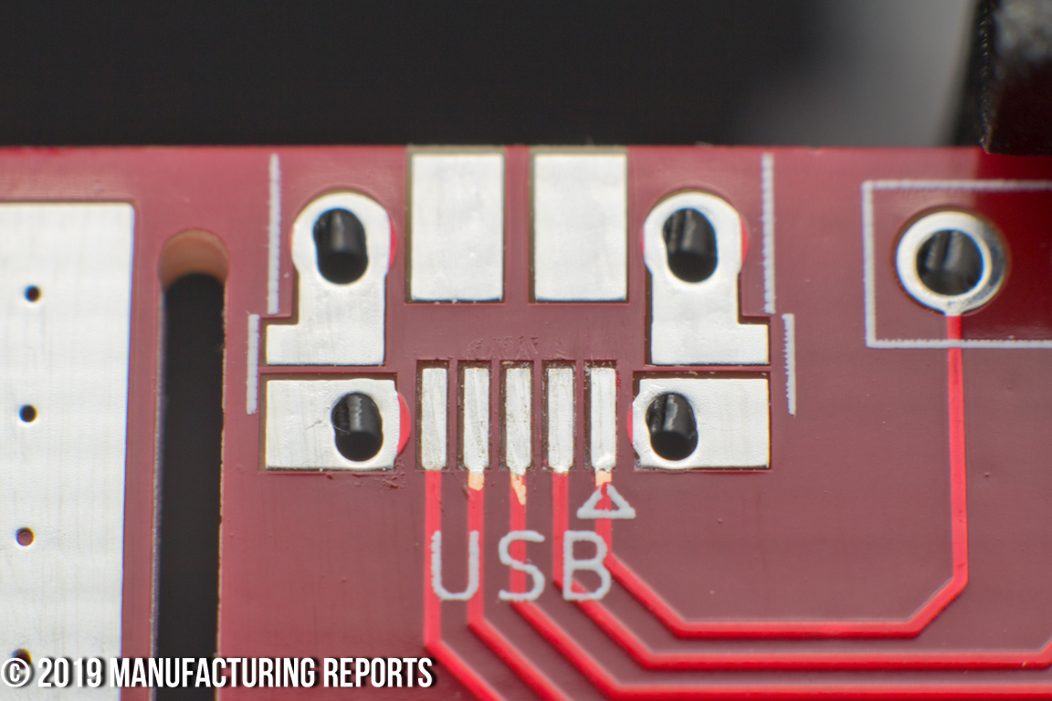
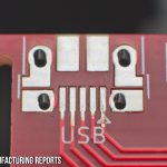
The HASL surface finish was complete across all boards, but in several instances the air blast failed to clean solder from several Micro USB Connector slots.
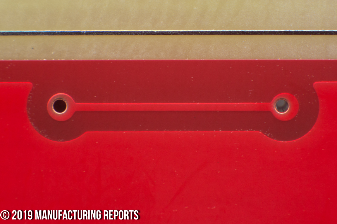
On the topic of the USB Connector, the footprints had significant issues. First, the footprint didn’t match the design file, as the location of the plated slots featured a circular pattern rather than the correct rectangular one. The slots themselves were far from perpendicular to the board edge, offset from 90° by anywhere from 15° to 45° in some cases. The position offset of the slots was also bad, cutting at the edge of the pad or off the pad on several of the PCBs.
-
- HASL Over Heatsink
-
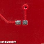
- 0201 Footprint
-
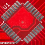
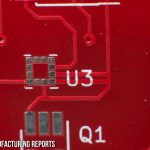
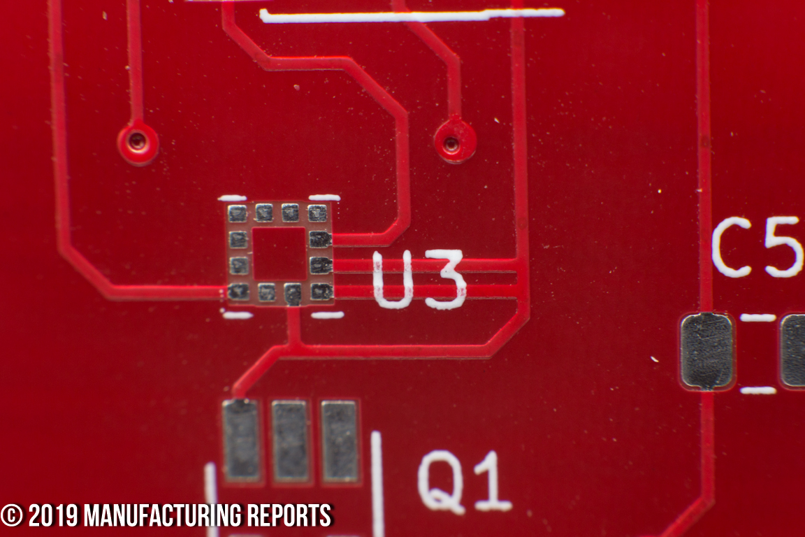
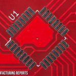
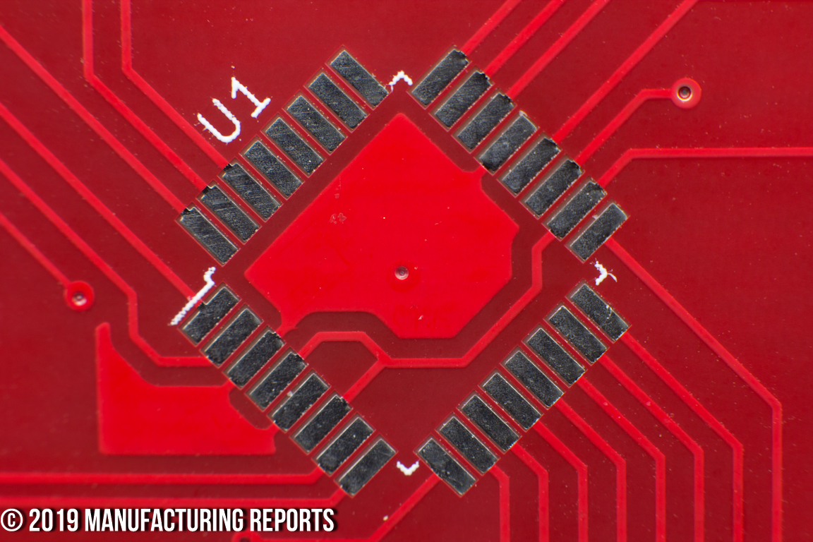
- QFP Footprint
-
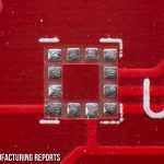
- QFN Footprint
-
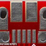
- Solder Clog Lower Left
-
- USB Connector Slot Offset
Solder Mask Quality
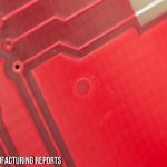
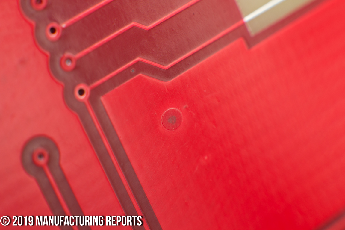
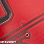
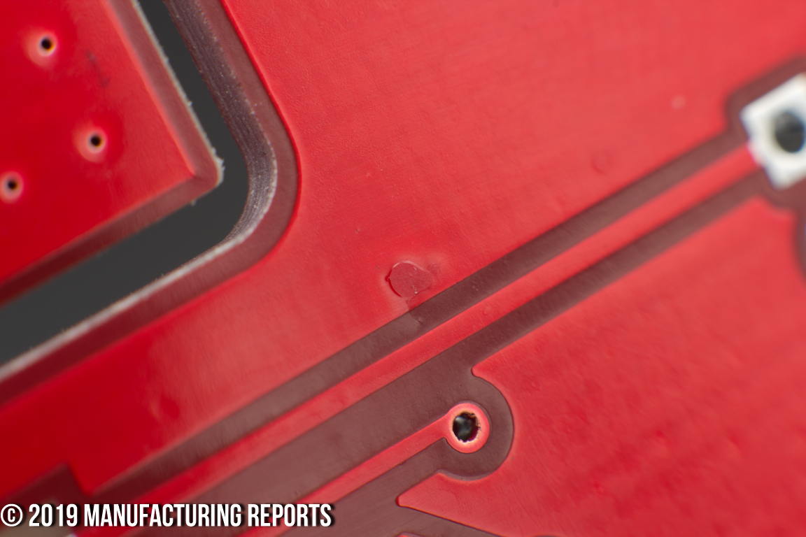
Due to the poorly applied, and un-requested, plating of the M5 mechanical holes, many of the boards had FR4 and plating contaminating the mask layer around the mechanical holes. Additionally, none of the boards escaped the factory without contaminants either on or under the mask layer, with chunks as large as 1mm trapped under the resist ink on some PCBs.
The registration of the solder mask was inconsistent, with some boards absolutely spot on — pads centered within their mask relief aperture — but some so offset that a hairline of the ground pour on the back side was exposed and conductive — the mask material coming off in thin strips.
While the via tenting was also inconsistent from the standpoint of completely encapsulating the vias, none of the annular rings tested as short circuits.
-
- Contaminant by Micro USB
-
- 1mm Diameter Junk
-
- Contaminant by Trace
-
- Inconsistent Via Tenting
-
- Large Offset
-
- Correct Mask to Pour Relief
-
- Nonexistent Mask Relief
-
- Exposed Ground Pour
Silkscreen Quality
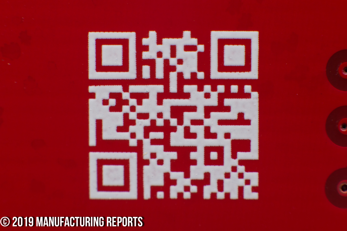
DirtyPCB states on their About page that the silk layer is applied through an actual liquid photoimagable process, rather than direct legend printing, and it shows. There was crisp detail inherent from the smallest passive reference designator at 0.5mm up to the full QR Code which was readable without magnification. Printing over varying z-heights was well accomplished.
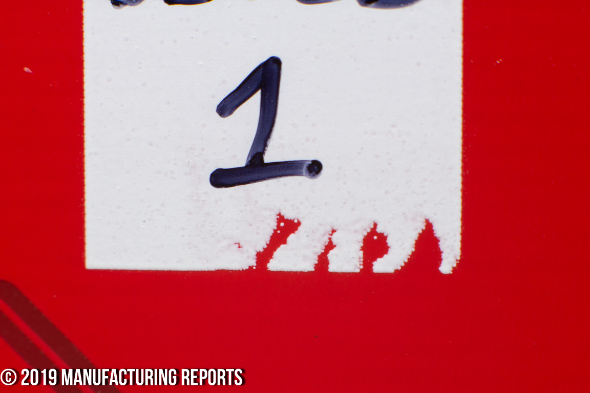
However, the beautiful silk layer was applied inconsistently. 60% of the boards had at least one misprint, where the ink either was never applied or peeled off prior to curing. In another case, the screen must have become clogged, causing the board name and design date to fade out slowly from one board to the next, to the next, until half of it disappeared entirely.
The Manufacturer’s Mark is printed on the face of the board in the upper right hand corner, as expected.
-
- QR Code
-
- Crisp 0.5mm Font Height
-
- 1mm Font Height
-
- Text Over Traces
-
- Good Board and Date
-
- Degrade Step 01
-
- Degrade Step 02
-
- Degrade Step 03
-

- Silk Layer Tear Out
Solderability
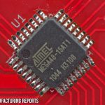
A board was chosen at random and subjected to two rounds of rework for both the QFP32 and USB Micro Connector footprints.
The QFP32 sat flat on it’s pads prior to soldering as the HASL was clean. Although there was some minor degradation of the solder mask leading from the pads up the traces after the initial soldering, the footprint ultimately held up well to the rework process, with only minor extension of mask erosion up the traces after both rounds. Oddly, I had trouble with solder adhering to the mask layer after the second rework — it didn’t pop off the resist as it usually does.
The Micro USB footprint suffered slightly more erosion up the traces through both rounds of the rework, although none of the mask web completely fell apart between the pads as happens with many other manufacturers.
The silk screen and solder mask never discolored.
-
- QFP32 Before Soldering
-
- QFP32 After Soldering
-
- QFP32 After First Rework
-
- QFP32 After Second Rework
-
- Micro USB Before Soldering
-
- Micro USB After Soldering
-
- Micro USB After First Rework
-
- Micro USB After Second Rework


