


Stackup
Stackup Definition
The stackup of a PCB defines the copper thickness, types of insulating substrates, number of layers of each and how they should be organized at the fabricator during manufacturing. Layer stackup is specified at the time of ordering, with the responsibility of layer material, thickness and order falling to the board designer to specify the materials and thicknesses they expect from the manufacturer.
Based on the desired electromagnetic characteristics the board designer may need to achieve, the way the various conductive layers are organized, or “stacked”, together with the different insulating layers, can help to protect sensitive signals travelling across or through the PCB. A well thought out design with appropriate layer organization can serve to minimize EMI as well.
Stackup Examples
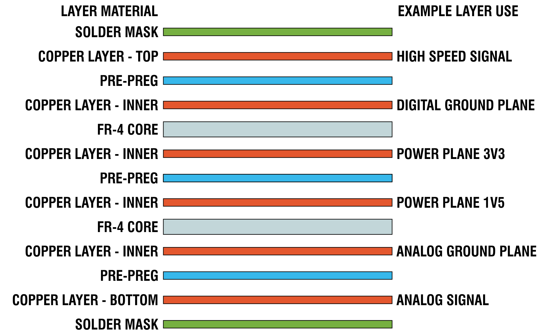
The most commonly manufactured board design is a four layer stackup. In a four layer printed circuit board, the two most inner copper layers are bonded directly to the FR-4 core material, with the outer copper layers then bonded through the use of a layer of prepregnated material.
Single and two layer boards also used regularly for low cost, prototype and simple designs. Higher layer counts are available for specialized applications involving high speed signal circuits or analog isolation, among others. Many power circuits in consumer electronics are located on very inexpensive single layer boards. In contrast, the main board in a modern television display may require 8 or 10 layers, while the printed circuit board in the remote control for that TV features two layers at most.
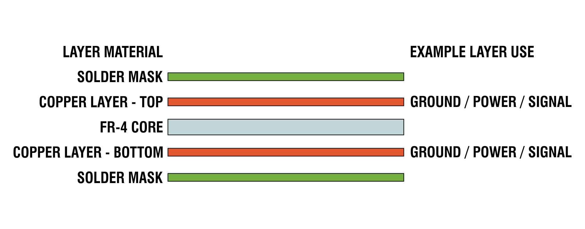
-

- Example of Two Layer PCB
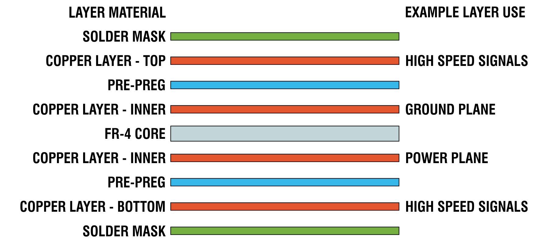
-
- Example of Four Layer PCB
-
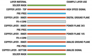
- Example of Six Layer PCB
For prototype orders, it is common to use a web interface to specify the layer arrangement, which tend to follow a similar look in feel across the industry. When placing orders for larger volumes or greater technical complexity, speaking directly a sales representative or sales engineer at the fab is highly recommended.


