JLCPCB PCB Service Review
JLCPCB
Shenzhen, China
$0.50
1 Day
2 Days
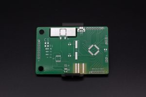
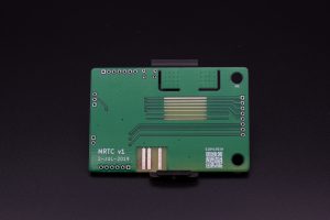
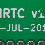
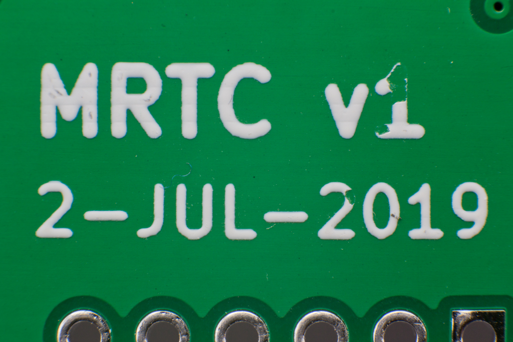
Manufacturing Reports Test Coupon v1
Lowest of the Low Cost Fabs
Good Ordering Options with Board Previews
Good Customer Service Experience
Manufacturer's Mark Can Be Relocated (not eliminated)
Rough HASL Finish
Solder Mask Overlaying Pads
Damaged Vias
Damaged Footprints
Solder Mask Erodes Easily During Rework
Order Delayed
JLCPCB, JiaLiChuang PCB, is the low cost king of the prototyping world, coming in at a frankly ridiculous $0.50 per board for 10 copies of the Manufacturing Reports Test Coupon. This JLCPCB PCB Service Review will show the quality of the business service and manufacturing capability of this Chinese manufacturer. They handle prototype orders with their factory in Shenzhen and production orders fulfilled by factories in Xinyu, Shuhai and Daya Baya, so I think it’s safe to say they handle a lot of volume, but does that volume come at the expense of quality.
Cost
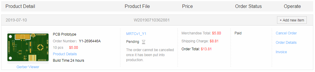
The total cost of the order for 10 copies of the Manufacturing Reports Test Coupon v1 was $21.81. As a new customer of JLCPCB, the current account activation email provides you with an immediate $8.00 shipping discount on your first order, and a pair of $5.00 off coupons for future orders. As those promotions only apply to the first few orders, I ranked the service based on that initial list cost, which was still the least expensive service of the 20 manufacturers I’m testing. The unit cost was $0.50 per board with $16.81 expedited shipping.
Ordering
Locating the design rules was as simple as searching Google for “JLCPCB Design Rules“, and returned their capabilities page.
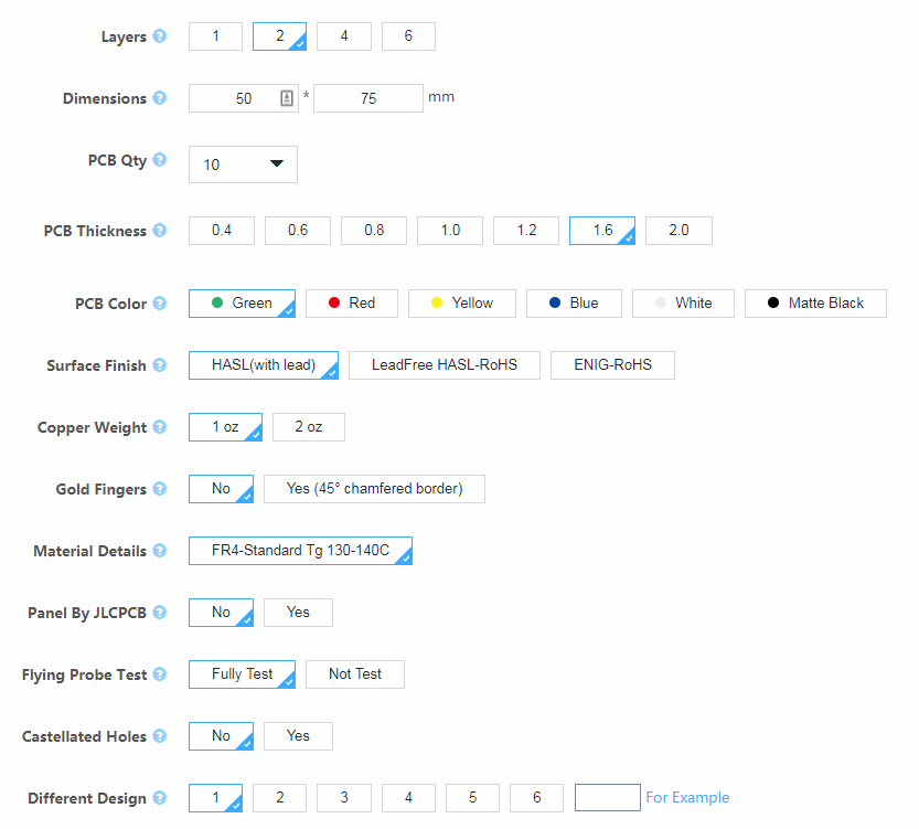
Prototype Service ordering options include 1, 2, 4 and 6 layer boards, in PCB thicknesses ranging from 0.4mm to 2.0mm in 0.2mm increments, 1.6mm being the standard. Boards must be ordered in multiples of 5.
After entering the generic specifications, we were brought to the detailed order page, and selected the recommended default stackup. Changing any of the basic settings results in either a delay or additional charge, as you would expect. For example, altering the default solder mask color would delay shipping by 3-4 days, and adding a RoHS compliant surface finish would increase the overall cost by $5.30 for Lead Free HASL and $16.30 for ENIG. The gold surface finish also incurs a shipping delay of 3-4 days.
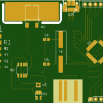
A board preview is shown before checkout, and suggested that the internal board slots around the via stitched heat sink would be manufactured, however their gerber viewer didn’t show them. Also not shown was the manufacturers mark that would appear above the lower right hand pin header footprint. No option is provided to eliminate the marking.
Looking around on their order support page, led to some general ideas around milled slots, but they seemed to be related to whether the slots should be plated or not. In my case, I submitted the order blindly to see how the factory would interpret the gerber files without any input from me.
Proceeding with those defaults, DHL 2-4 day service was selected rather than the registered mail option of 15-20 business days. Expedited shipping was an additional $16.81.
-
- JLCPCB Ordering Options
-
- JLCPCB Sales Preview
-
- JLCPCB Gerber Preview
Fulfillment
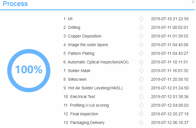
For this review, DHL 2-4 Day Service was selected and the order placed on 10-Jul-2019.
Unfortunately, the order seemed to go into limbo. No update emails were sent, even though the official “Order Process” window seemed to indicate that the order had been sent to “Packaging/Delivery” in the morning. After waiting an additional 24 hours an email was sent to support asking for the order status. They responded within an hour (around 7AM on a Saturday in China) and acknowledged that the order hadn’t shipped, and that the customer service representative would investigate. Two hours later, a shipping notification was emailed with a DHL tracking number.
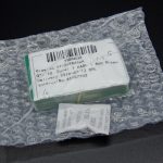
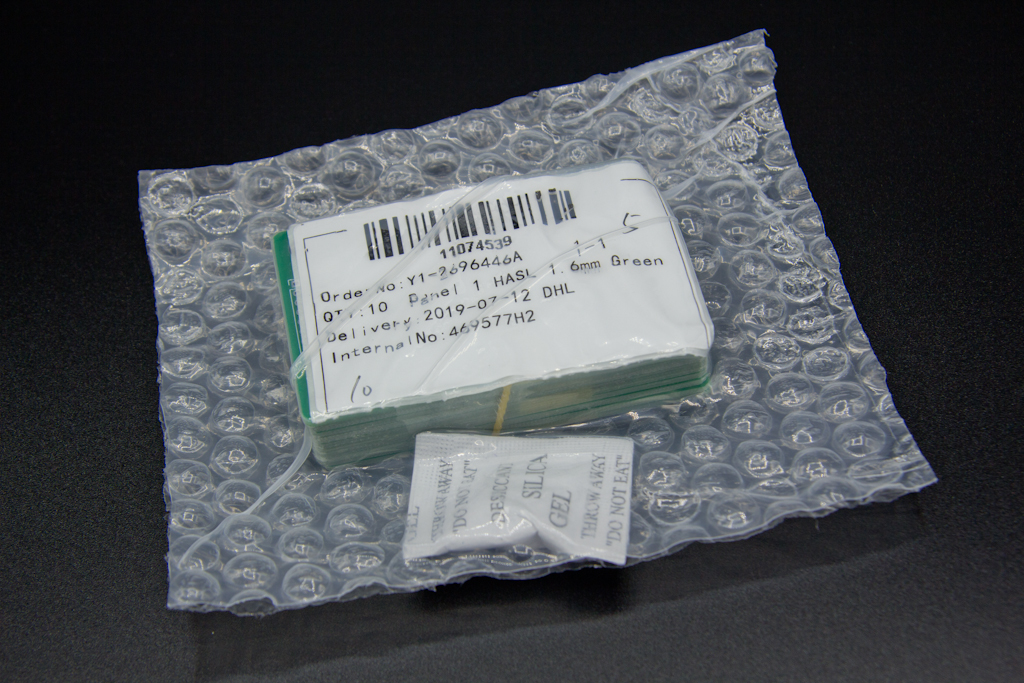
The boards arrived in five calendar days inside a standard DHL shipping pouch, containing a JLCPCB branded cardboard box, nicely filled with bubble wrap. The PCBs were stacked and packed with silica gel in a vacuum sealed bubble pouch as well. As a nice little treat, a little magnifying bookmark was included.
-
- Production Progress
-
- JLCPCB Order Packaging
Customer Service
No order confirmation email was sent after placing the order, however the payment page was replaced by the order status page associated with my JLCPCB account. That page shows the current manufacturing status, and indicated the order was paid with a link to a cleanly generated HTML invoice.
An email was sent to their general support address asking for a PDF copy of the invoice. The email was sent at 12:08AM in Shenzhen so an immediate response wasn’t expected. At 07:46AM Shenzhen time, they responded stating that an invoice could only be generated by their system after shipping, so please use the order page to download a copy, which I felt was fair, and an excellent response time.
Order Status
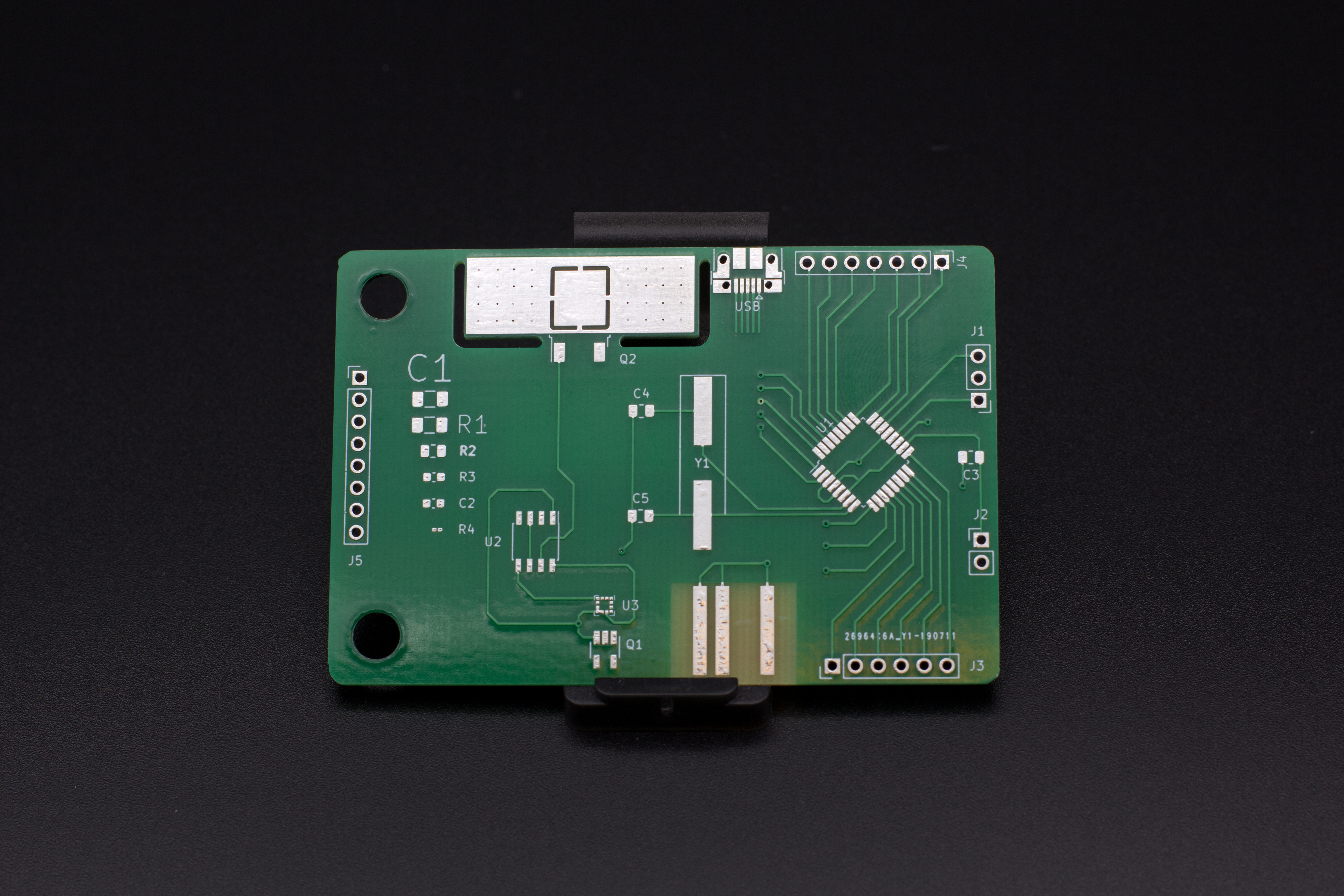
Circuit Board Visual Inspection
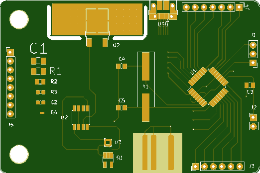
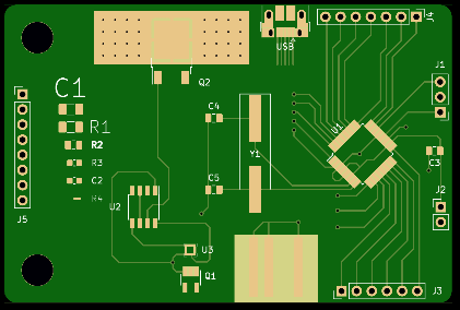
-
- JLCPCB Full Board Front
-
- JLCPCB Full Board Back
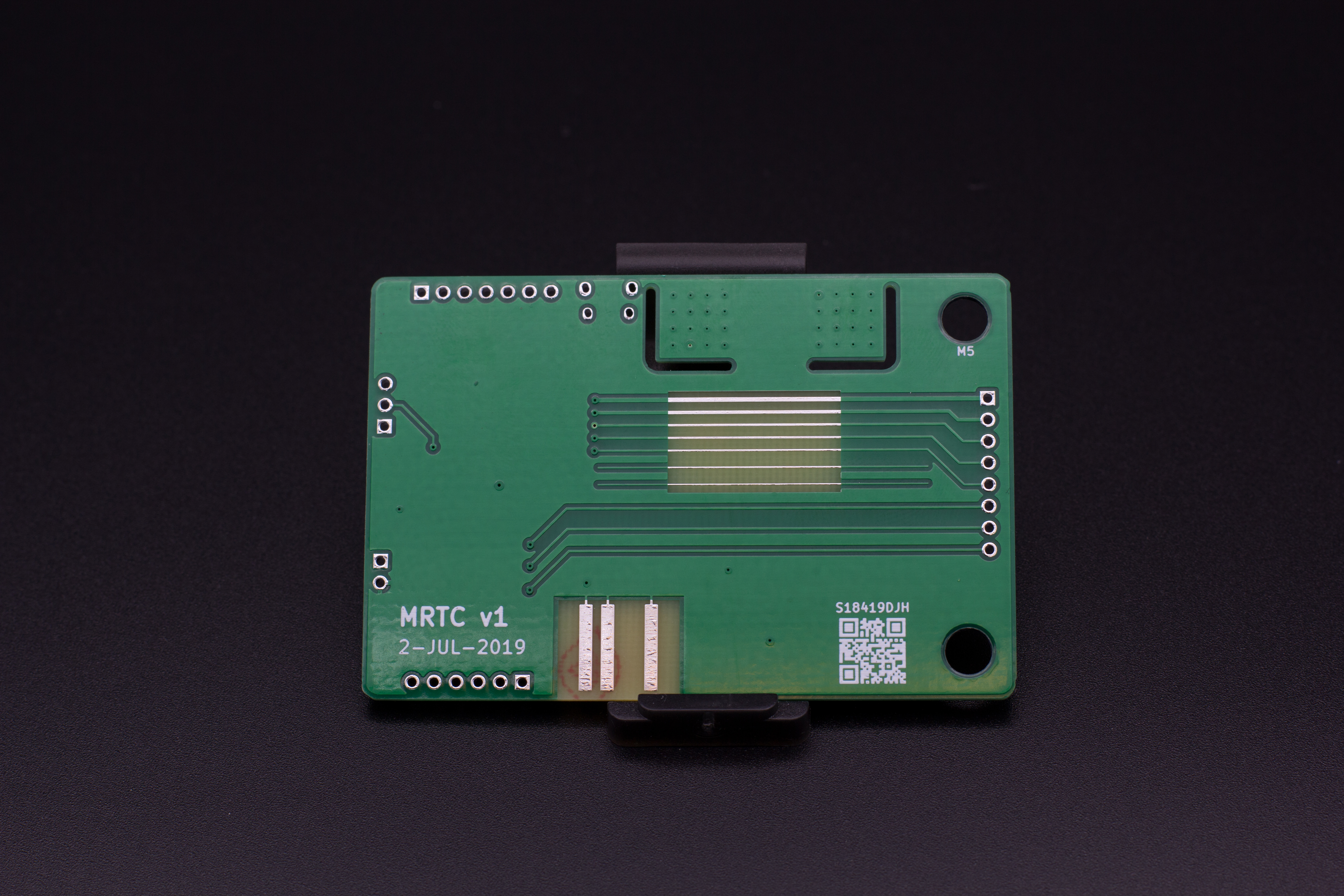
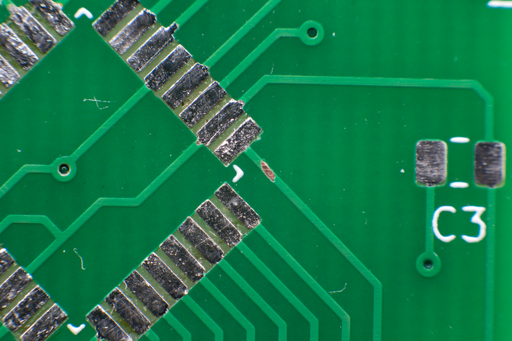
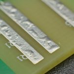
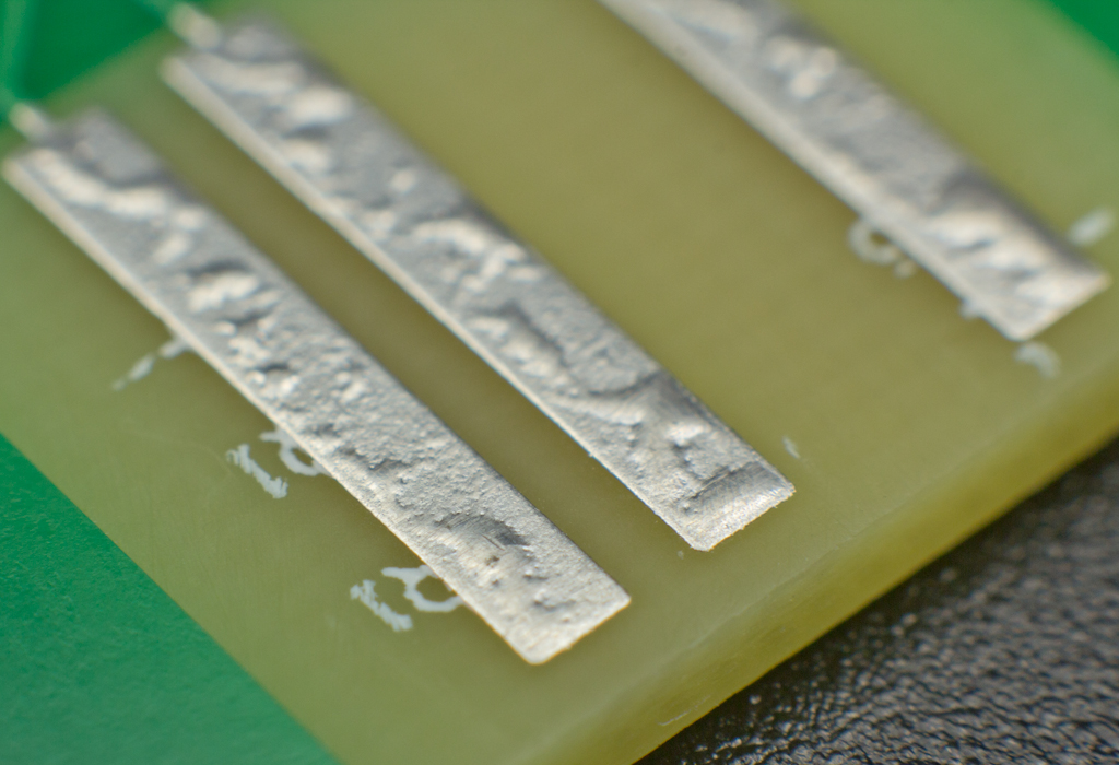
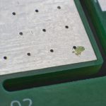
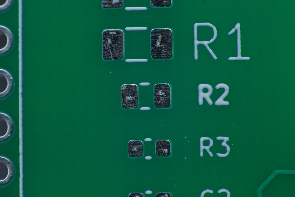
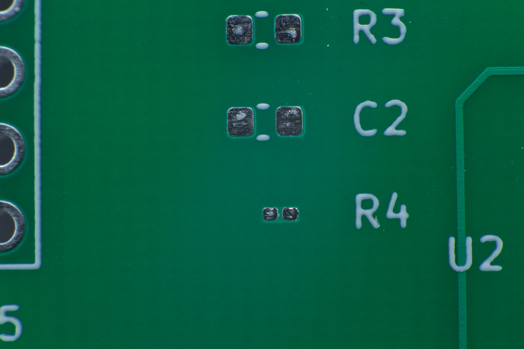
Straight away, two of the boards had unusable 0201 footprints, with one board missing both pads, and the other having only a single damaged one. At first glance under an inspection lamp, the board edges were cleanly milled, with no hint of mouse bites. Drills seemed good and the internal slot was fabricated correctly.
Beyond that, though, I was surprised by inconsistencies. While many of the problems I found would seem to be minor imperfections, every board had one, and they seemed unique from one board to another. Bad silkscreen, damaged vias, inconsistent copper pours and simple manufacturing mistakes were all present. That so many different problems could appear in a single order of ten boards gives me pause.
PCB Dimensions
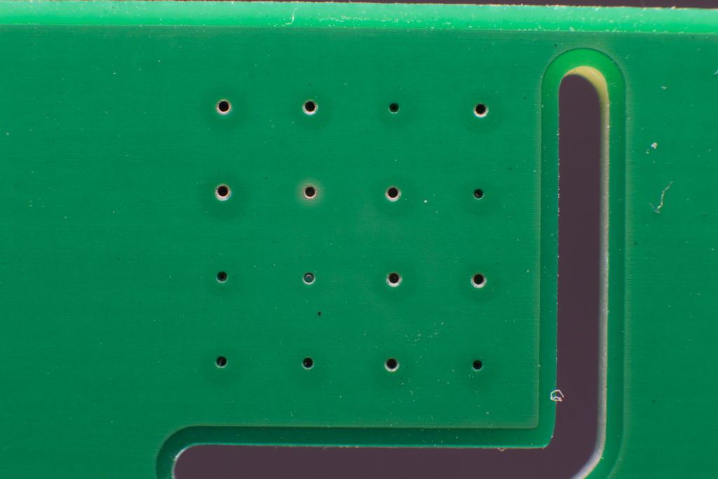
The board edge dimensions measured well within tolerance, tending towards undersized by a few hundreths of a millimeter. The board thickness was also within tolerance across all boards, again, with all boards slightly undersized and the thinnest measuring 1.54mm against the 1.6mm standard. The internal slot around the heatsink area was milled, and measured to spec. Trace widths were exactly defined in the design files.
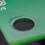
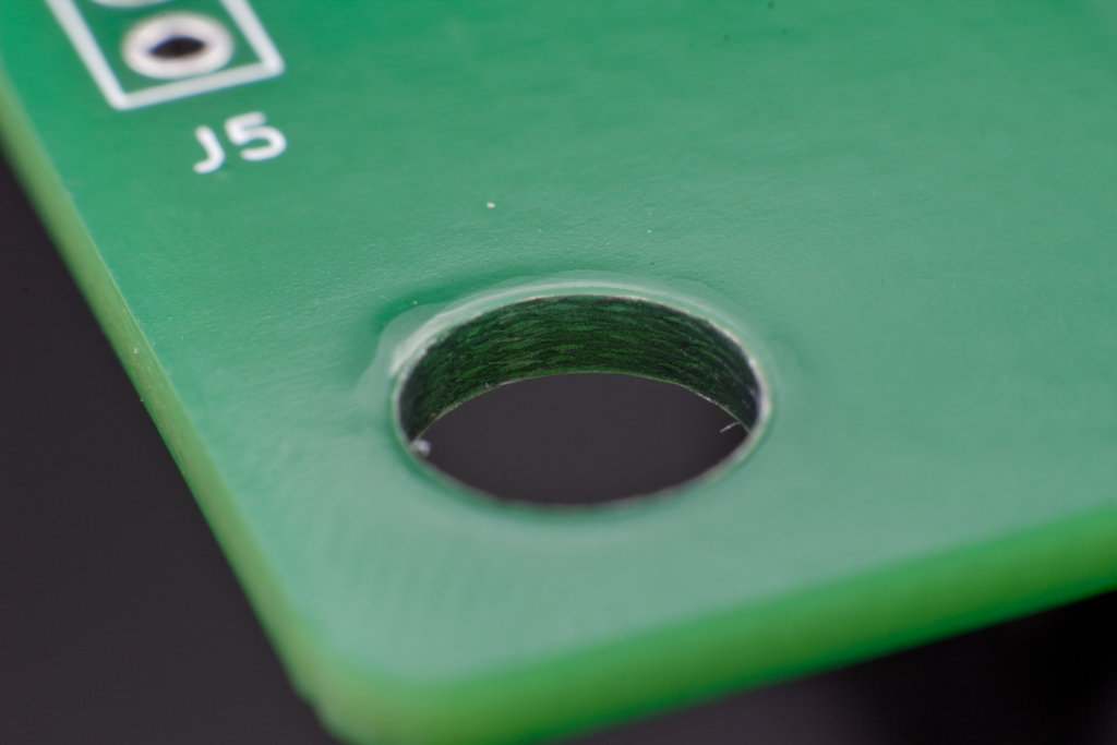
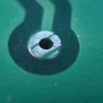
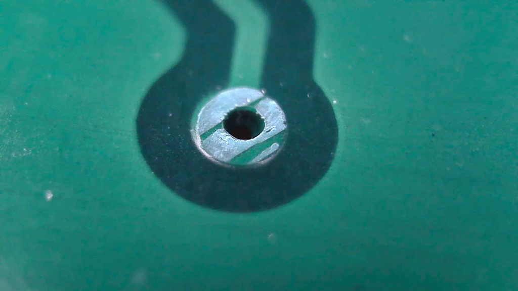
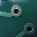
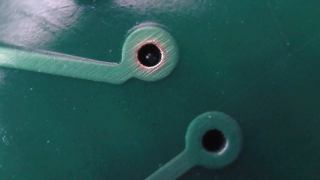
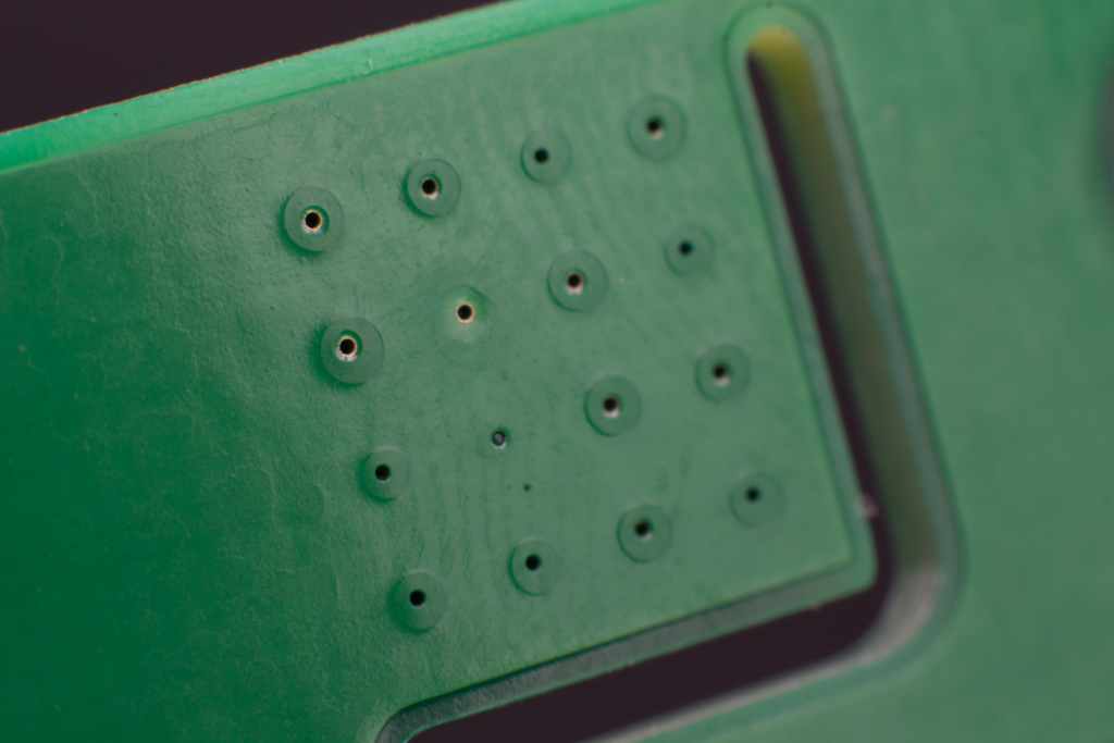
The M5 clearance mechanical NPTH all measured within tolerance and positioning of those features fit the test jig with no problem. I did notice that the milling process that formed the holes raised a visible burr around the edges that wasn’t removed, and the factory just applied the solder mask over it. The inside of the hole looked very dark, too, and I suspect there was some problem during milling with either a dull endmill burning the edges, or some system not cleaning the milled chips out resulting in excess heat, rather than cutting cleanly.
There were slight offsets on the backside of several boards with the via drills. The vias are 0.4mm drills (15 mil) with 0.8mm (31 mil) annular rings, so there is a bit of meat to play with, but not much. The offset was never so large as to completely hit the edge of the pad, they simply were visibly off center.
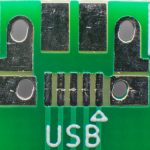
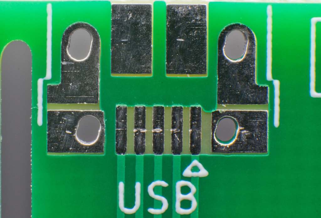
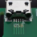
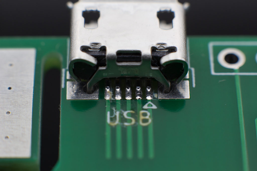
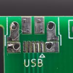
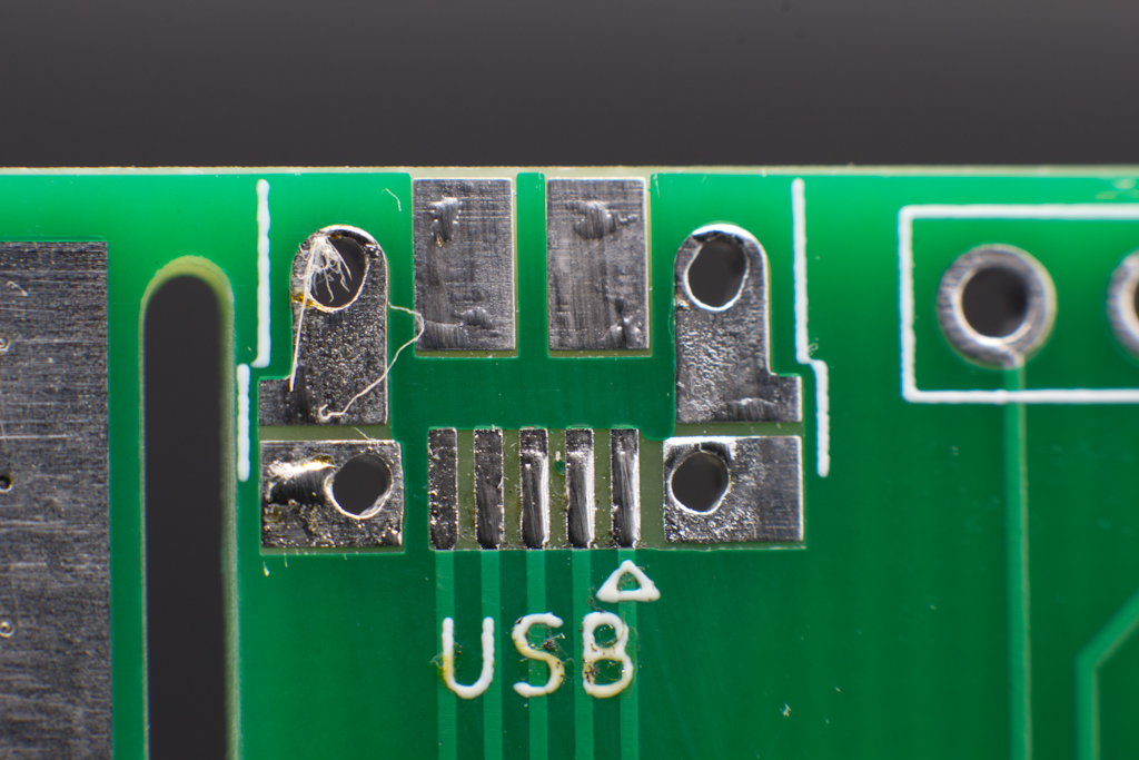
The milled and plated slots for the mini-USB footprint were skewed on all boards and not perpendicular to the board edge.
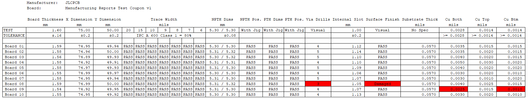
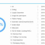
JLCPCB Test Report for 2019
-
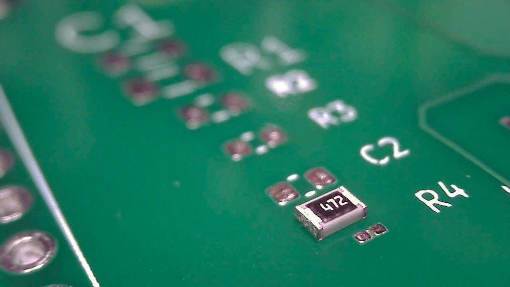
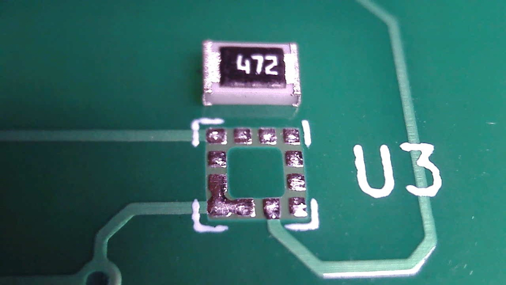
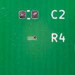
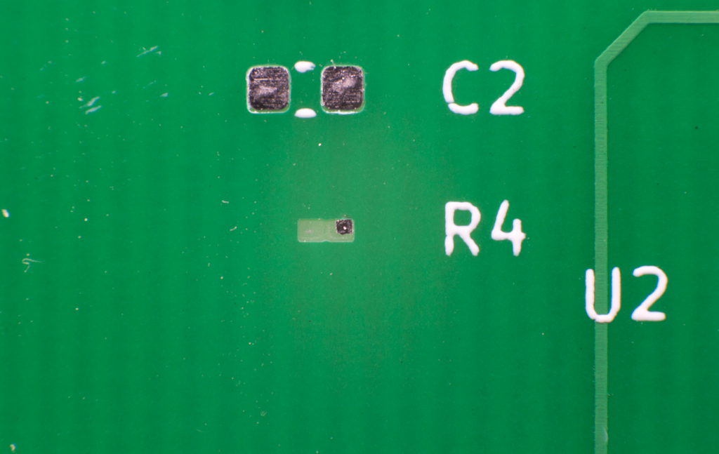
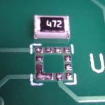
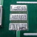
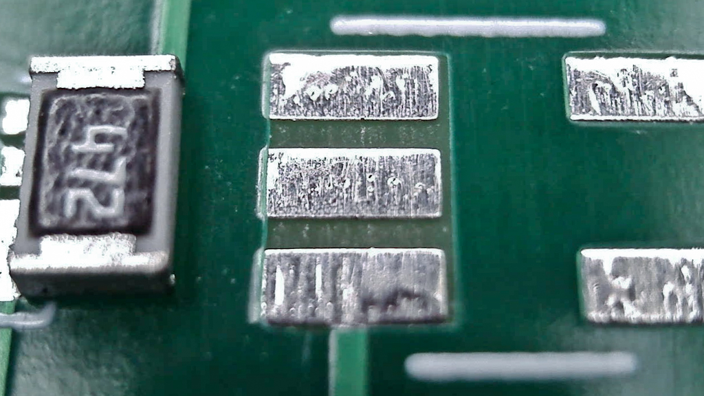
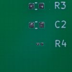
- SMT Passives Footprints
-

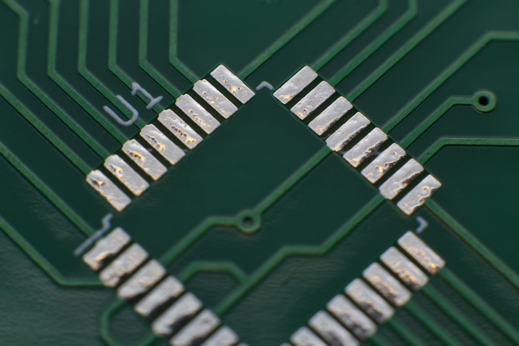
- QFN Footprint
-
- Burr and Scorching of NPTH
-
- Skewed Plated Slots
Copper Layer Quality
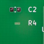
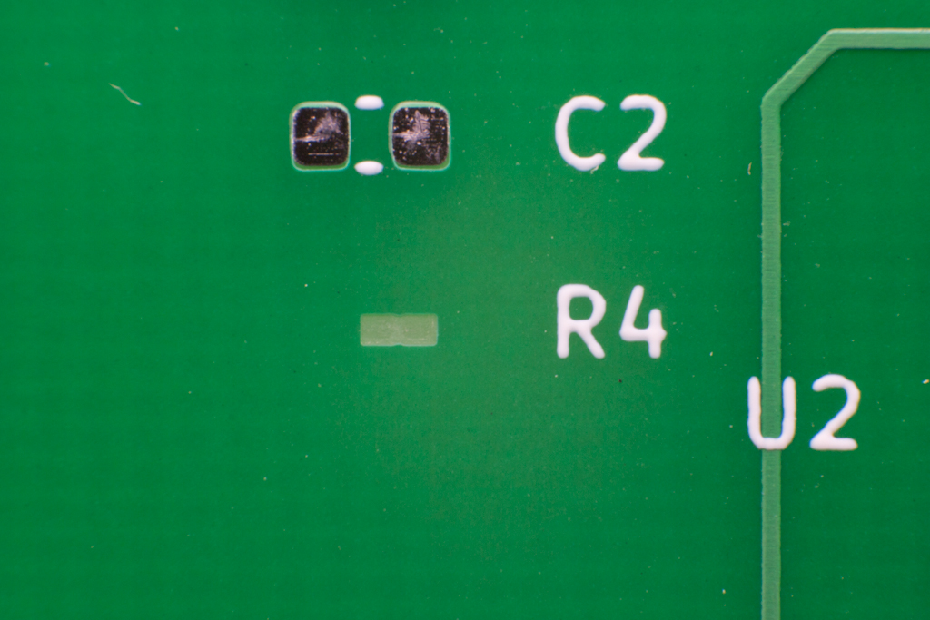
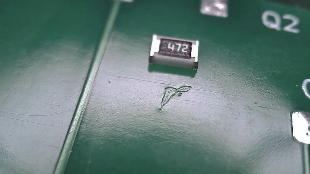
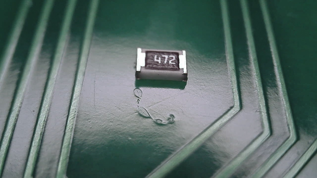
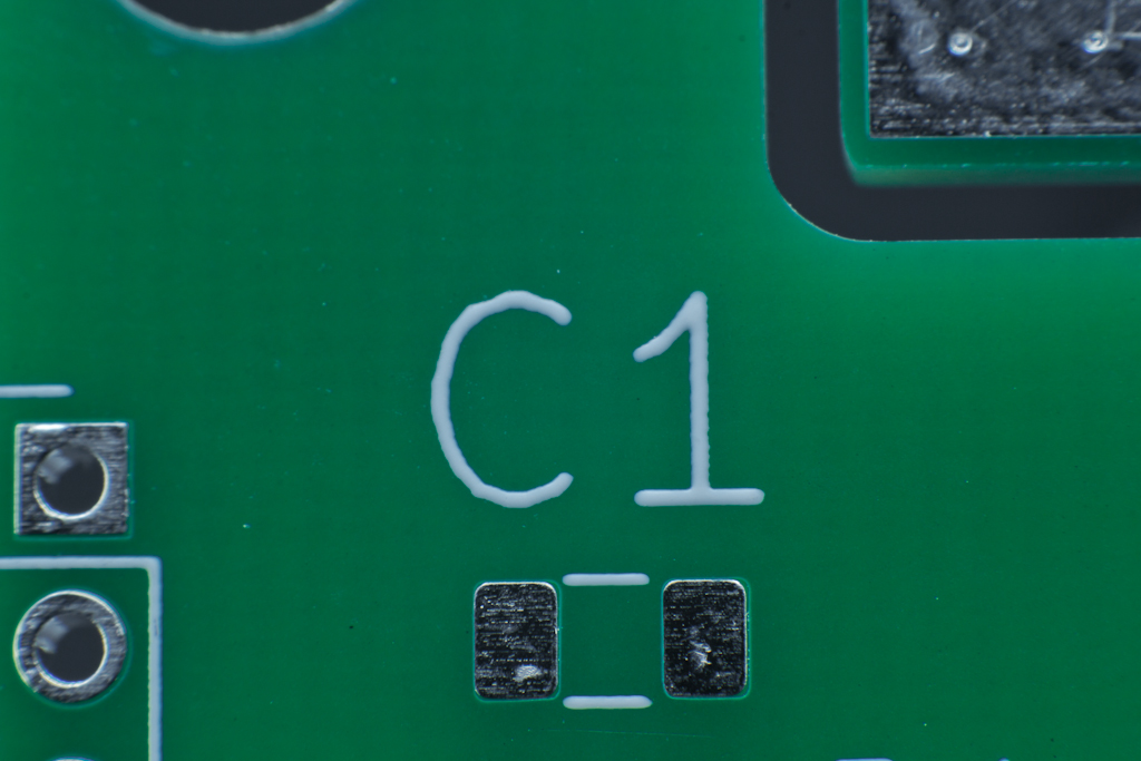
As mentioned above, on two boards the 0201 footprint was either completely missing its pads, or only had a single pad, rendering those boards as failed. That’s completely unacceptable because JLCPCB states in their FAQ on E-Testing that “All PCBs undergo a 100% AOI (Automated Optical Inspection) to make sure that all tracks and pads are connected.” If you’re performing optical inspection along with flying probe, there’s no reason you shouldn’t pick up an entirely missing footprint.
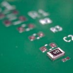
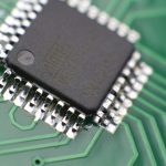
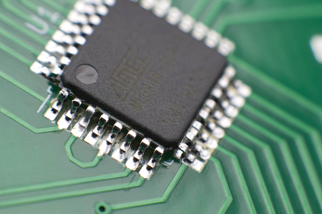
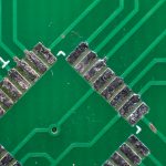
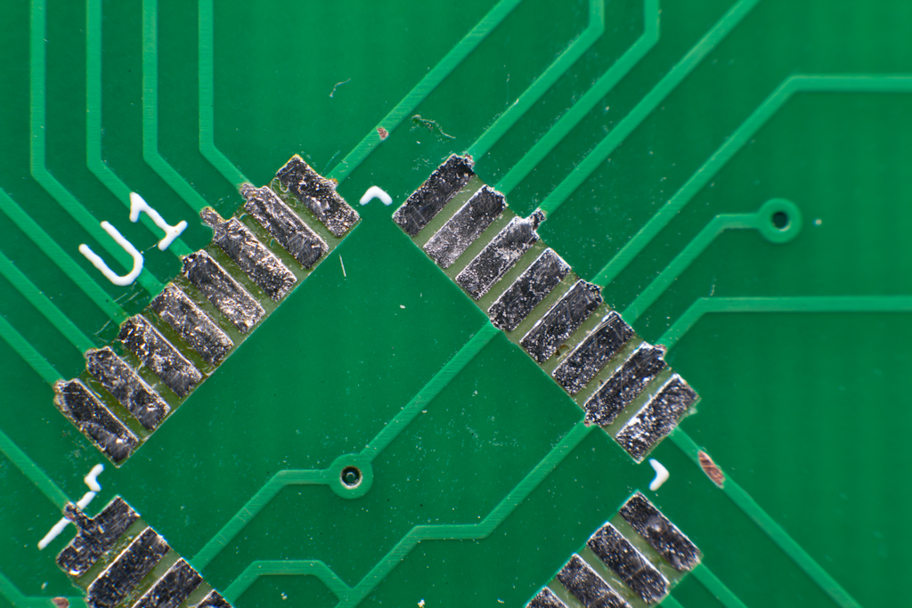
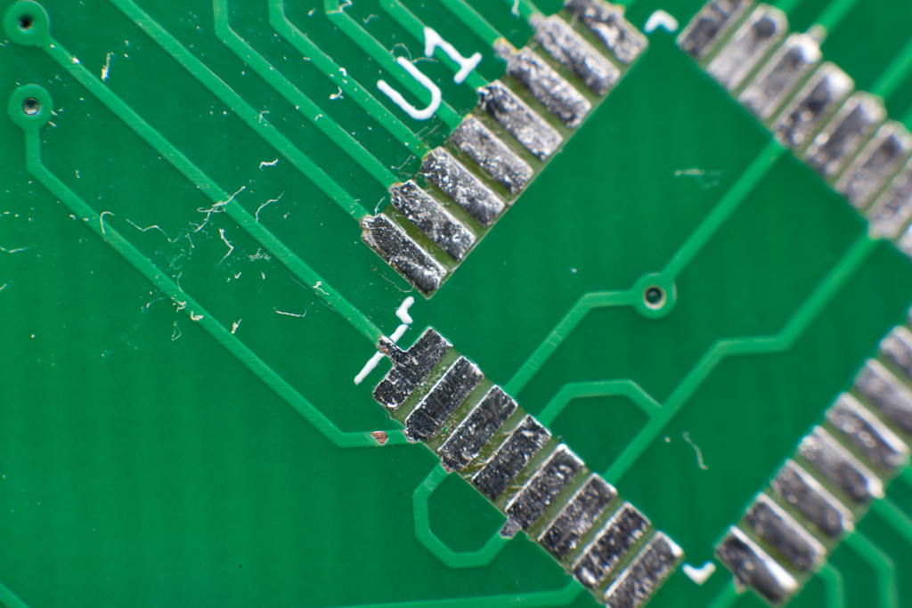
Universally, the QFN and QFP footprints were fabricated with good quality and no issues. The QFN in particular were good to see, as HASL really isn’t the best surface finish for pin pitches that small.
The boards all tested correctly to 1oz copper thickness but the HASL surface finish was consistently rough. In the heat sink area of one board, the HASL and copper was scraped away somehow, exposing bare FR4 underneath.
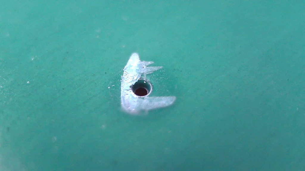
One board had damaged vias on the back side copper layer, with significant scraping across the surface having occurred.
Yet another board had a strange silkscreen overprint, that seemed to have happened after the solder mask was applied but before the HASL process. If the solder layer hadn’t been applied we’re certain there would have been ink across the pads in the thickness testing area.
-
- Silkscreen Overprint
-
- Missing 0201 Footprint
-
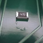
- Damaged 0201 Footprint
-
- Damaged Via 1
-
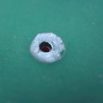
- Damaged Via 2
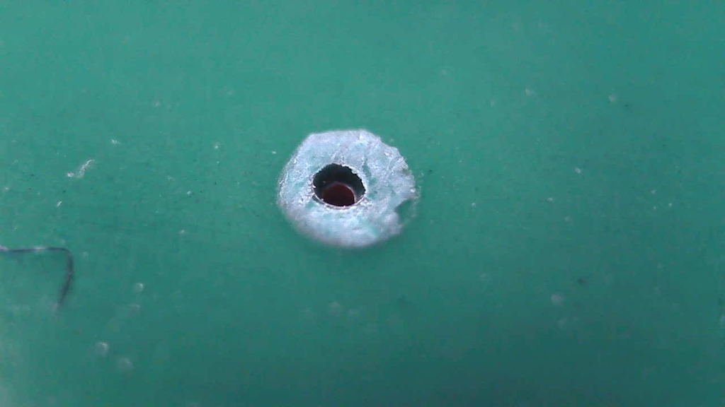
-
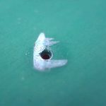
- Damaged Via 3
-
- Damaged HASL and Copper
-
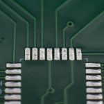
- QFP Footprint 01
-
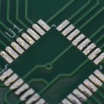
- QFP Footprint 02
-
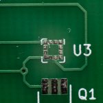
- QFN Footprint 01
-
- QFN Footprint 02

Solder Mask Quality
The solder mask seemed very thin in areas, and particularly around the backside copper of the heat sink. There were also odd raised areas in the back side solder mask around the majority of the vias that at first I though was because of the via’s annular ring, but after thinking about it for a moment, realized that those were vias straight into the ground plane, and that means there is no annular ring on that side.
On some of the boards, there are particles of some contamination embedded under the solder mask.
Looking at the pads under the microscope, it was clear that the mask layer was offset far enough to overlay the pads in several cases, rather than having a clear separation around the solder points.
-
- Solder Mask Offset over SOT23-5
-
- More Contaminant Under Solder Mask
-
- Contaminant Under Solder Mask
-
- Scraped Solder Mask
-
- Solder Mask Thin at Via Stitching
-
- Solder Mask Quality at Via Stitching
Silkscreen Quality
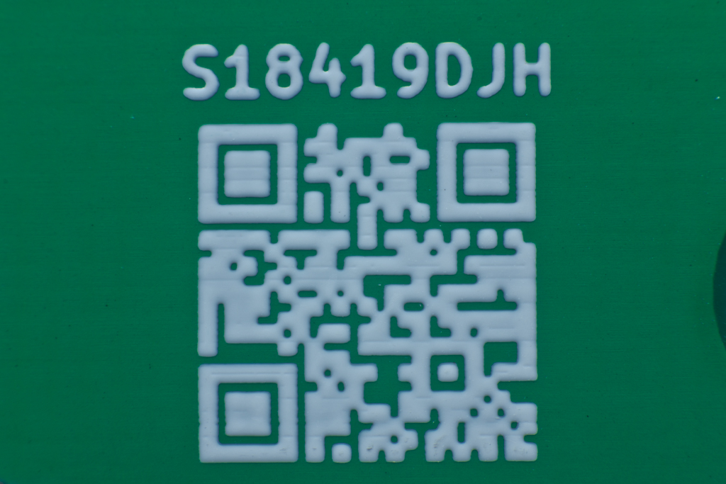
The silkscreen is of a low resolution printed type, which I expected from an inexpensive prototyping service. The QR code doesn’t resolve on any board even with magnification.
When applied correctly, the text on the silk layer is perfectly legible from the largest to the smallest fonts. However one board had a printing glitch that affected the quality of the board name on the back side silk layer.
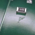
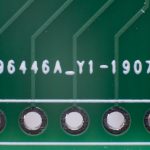
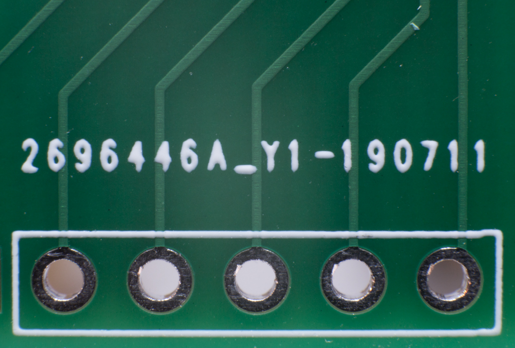
A manufacturer’s code was printed on all boards above the J3 connector. I expect this from off shore manufacturers, not that I like it, and there wasn’t an option during the order process to eliminate it. I would have preferred that the code be printed on the backside though, rather than prominently on the front, or within the footprint of a larger component so the graphic is hidden after assembly.
-
- Silkscreen Quality Passives
-
- Silk Screen Quality
-
- Silk Screen Passives 01
-
- Board Name Damaged
-
- JLCPCB Manufacturers Mark
-
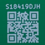
- QR Code Resolution
Solderability
The QFP and USB Connector were hand soldered in place using the drag soldering method. Both components soldered down easily, presenting no problems with alignment along any axis, and sat flat against the PCB before and after assembly.
The USB connector cleaned up easily during rework, and didn’t show any sign of solder mask erosion. The silk layer didn’t suffer from the rework either.
The QFP pads did not lift during two reworks of the chip, and the pads remained undamaged. However, after the cleaning the pads with solder wick , I saw erosion of the solder mask beginning at several locations around the QFP, exposing the traces underneath. Each exposed trace tested conductive to it’s connected pad using a DMM. After subsequent rework cycles, I noticed that the solder on the pads was starting to crawl up the as the solder mask eroded further.
-
- QFP32 After Initial Soldering
-
- Micro USB Connector Initial Soldering
-
- Micro USB Connector After Rework
-
- QFP Solder Mask Erosion After Rework
-
- Solder Mask Damaged After QFP Rework
-
- Solder Mask Damaged After Rework