Smart Prototyping PCB Review

Smart Prototyping
Hong Kong
$0.99
7
3
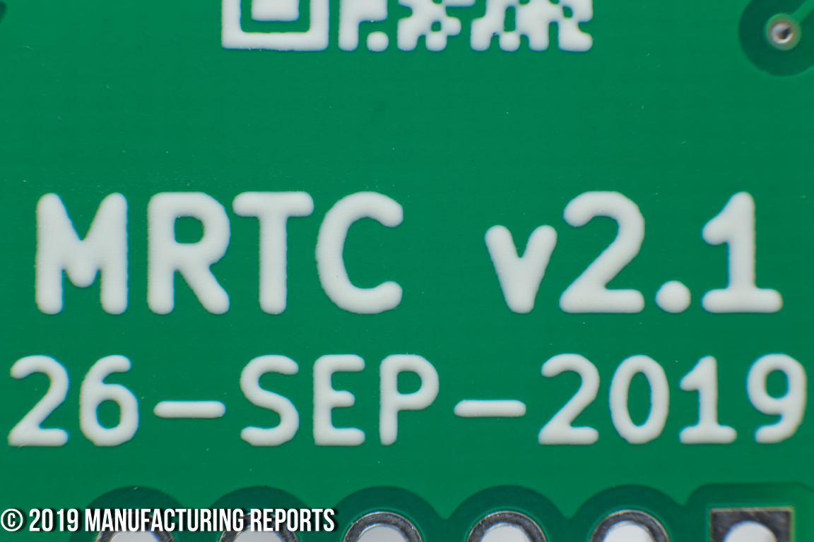
MRTC v2.1
Exceptionally Clear Ordering Options
Good Customer Service Response Times
Shipped Before Holiday Deadline
No Board Damage
Good HASL
Several Boards with Perfect Via Drills
Strong Resilience to Rework
Slight Shopping Cart Hiccups
Design Rules Hard To Read
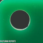
Poor Milling Tolerances
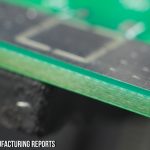
Very Thin Solder Mask
Some Solder Mask Contamination
Smart Prototyping, also known as NOA Labs, is a PCB fabricator and EMS located in Hong Kong and Shenzhen. Like many of their competitors, they provide a market place for the sales of open source hardware developed in-house and sold under the Zio and Qwiic brand names. While it has absolutely nothing to do with manufacturing, I was very happy to see that they actually published the design files and specs for their open source hardware on the Zio Github page.
Cost
As another relatively low cost fabricator, Smart Prototyping came in at $9.90 for 10 boards, 0.99USD per unit. This is the same per unit ball park as Shenzhen2U and ALLPCB. However, they charge a whopping $28.79 for DHL Express delivery, which is nearly $10 above the average I track for offshore fabs ($19.64). No additional fees were applied.
Ordering
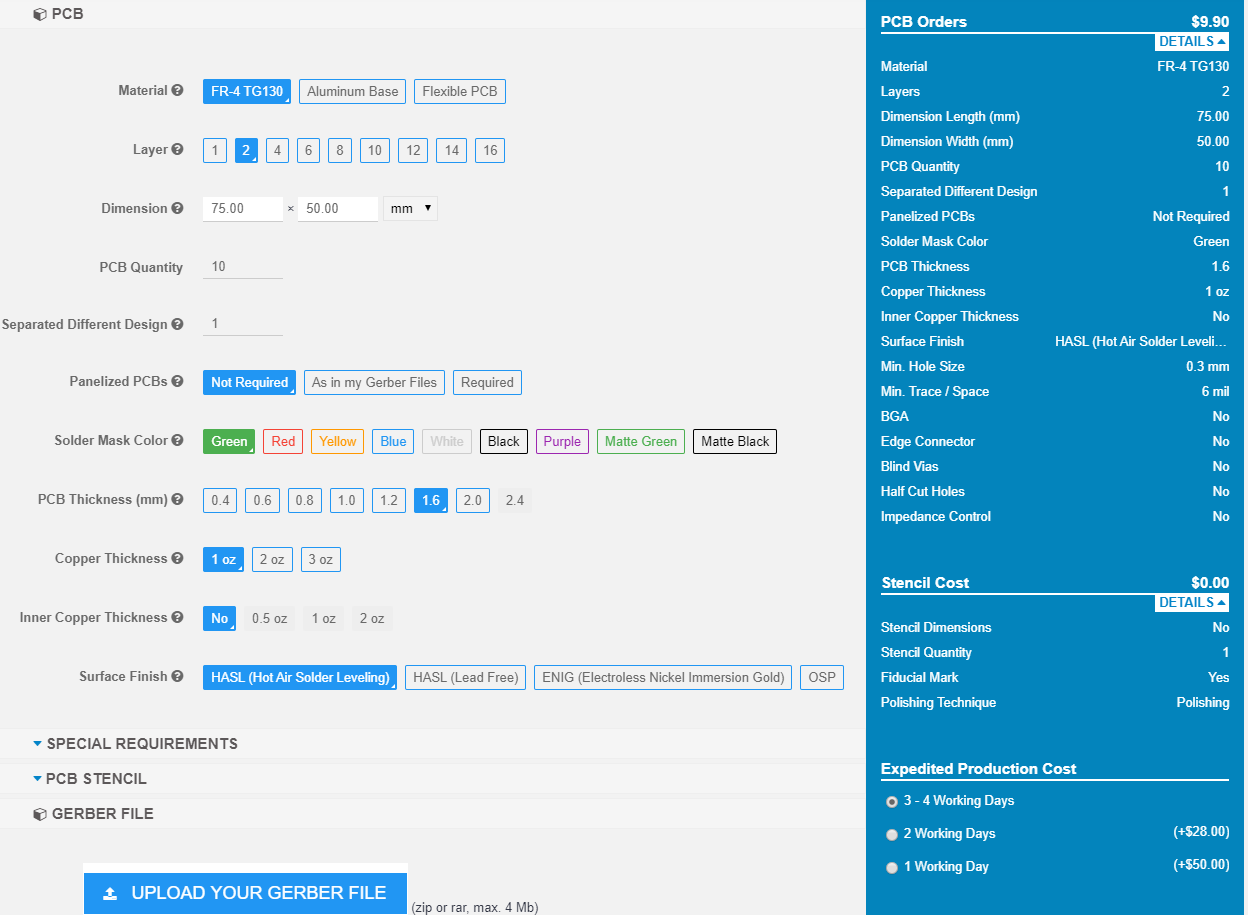
I really found their ordering page for prototype PCBs very clearly laid out. The dimensions and stackup options necessary for a basic quote are laid out right away, with more advanced features underneath accordion menus on the same page. As you make changes to your specs, the quote updates right away to let you see the difference between the options in terms of cost and delivery times.
For purposes of ordering the MRTC v2.1 no special requirements or PCB stencils were selected. No option was available to prevent printing of a manufacturers mark, and no mention is made if that will appear on the board.
I did have some confusion, that after selecting the order options and uploading the Gerbers, I clicked “ADD TO CART” and nothing happened. The screen just auto-scrolled back to the top of the page but no indication was given to suggest the order was registered in the cart. Clicking on the little shopping cart icon showed that the 10 board order had been registered in the cart each time I’d clicked. A little clean up of the quantity, and the necessary creation of an account on their site, had the order ready to go. 2-3 Day DHL shipping was applied to the order an payment processed by PayPal.
-
- Ordering Options
-
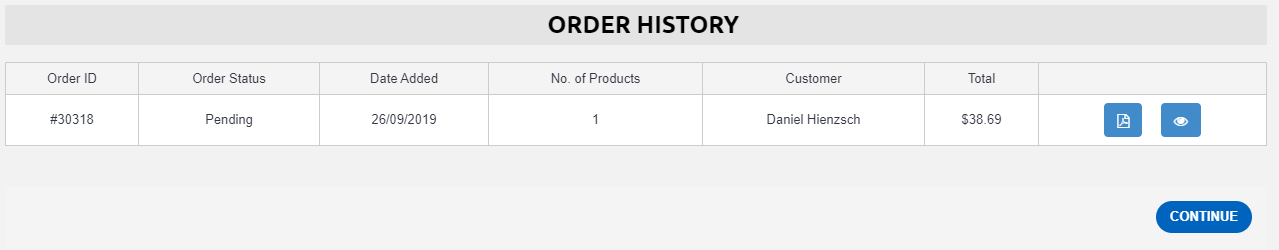
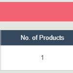
- Order Status
Fulfillment
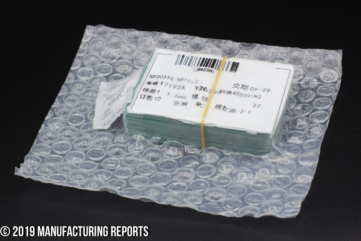
These boards were very well packaged in a hard cardboard box, with bubble wrap inside and then the standard vacuum bubble pouch surrounding the boards with a little sachet of desiccant nuggets.
-
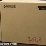
- Fulfillment Box
-
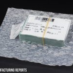
- Standard Vacuum Bubble Pouch
Customer Service
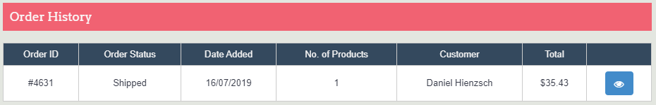
Immediately after ordering, a very clean email order confirmation was received with an attached PDF invoice. The order was available for viewing in the order history section of the customer account page at the Smart Prototyping website, however the order status was very sparse merely saying “Pending”. In fact, other than color scheme, the order status page looked remarkably similar to that of ShenZhen2U.
An email was sent asking for confirmation of what I should expect for a shipping date, as they publish a “2-3 business day” turn time for standard prototype orders and I was up against the Chinese Golden Week holiday. A few hours later, I received a response explaining the shipping lead times and that I would most likely be impacted by the holiday and the boards would ship afterwards. However the boards shipped the Saturday before and arrived the following Wednesday.
Design rules for Smart Prototyping seem a bit of a mess to decipher. I wasn’t able to fine a PDF or table of rules or tolerances outright, but on the Smart Prototyping FAQ page, they have an accordion menu with items such as “What is the milling diameter tolerance?” or “What is the minimum trace width of 2oz copper thickness PCB?”
-

- Smart Proto Order Status

-
- Shenzhen2U Order Status
Circuit Board Visual Inspection
-
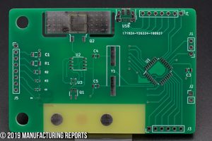
- Smart Prototyping Review Full Board Front

-
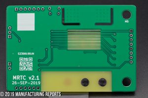
- Smart Prototyping Review Full Board Back

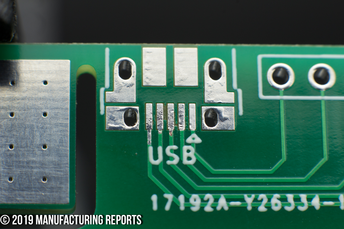
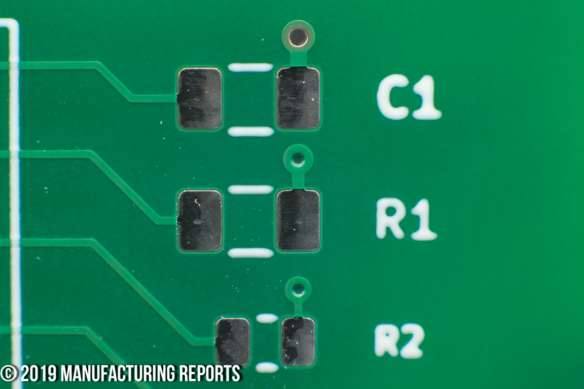
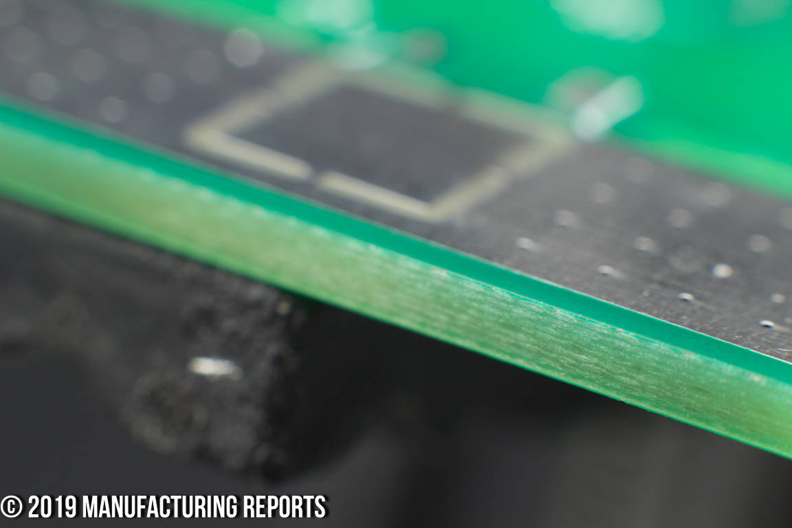
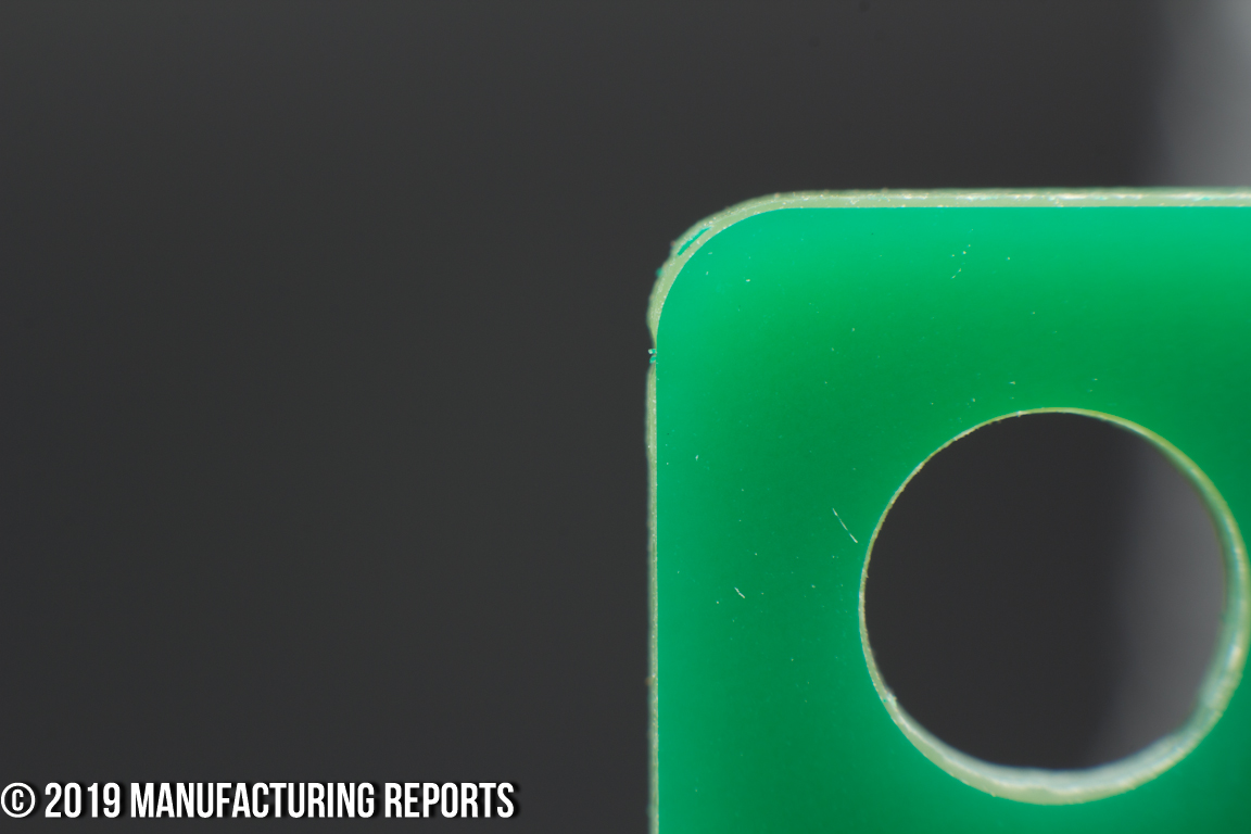
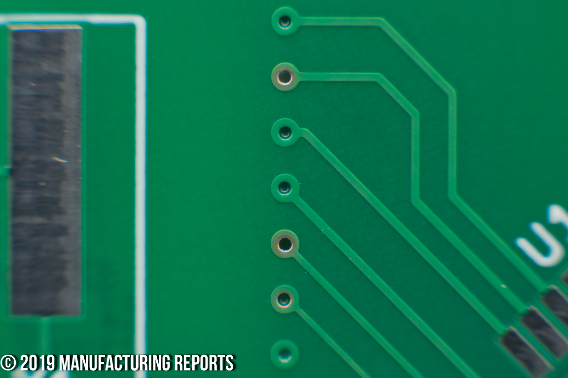
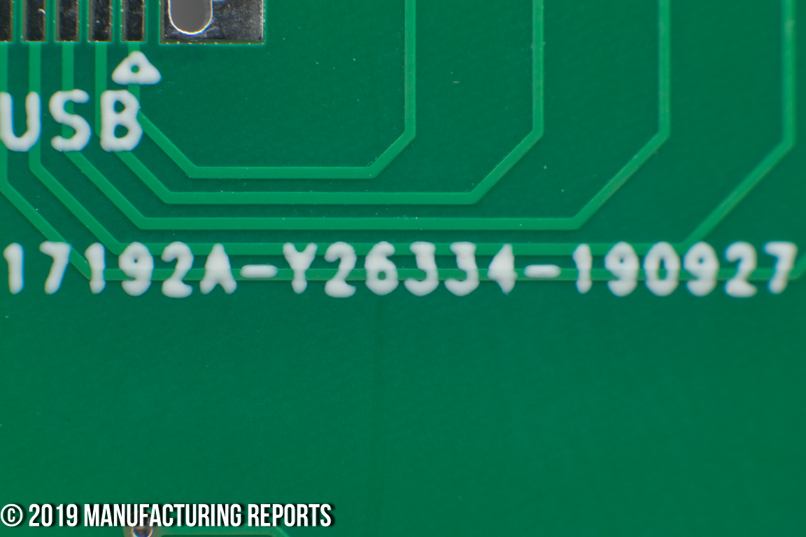
These boards must have come from the exact same fab as the ones in the ITEAD PCB review as they showed all the hallmarks of whatever factory that is. The mechanical holes were immediately suspect as they looked very poorly milled even without the inspection lamp. The solder mask is obviously thin, to the point of many vias being exposed with the “Kingboard” logo on the substrate being easily visible. The surface finish of the pads looked good, if not as super clean as other boards, and the plated slots were straight, but not exactly perpendicular.
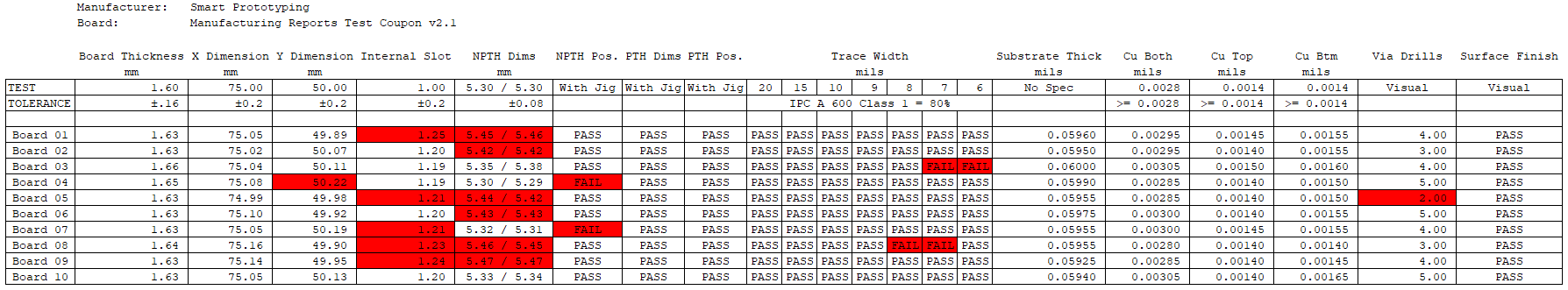
PCB Dimensions
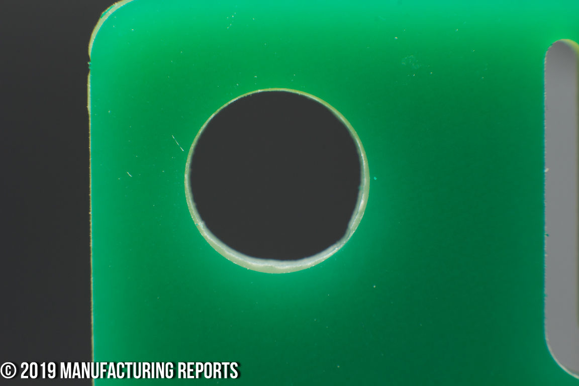
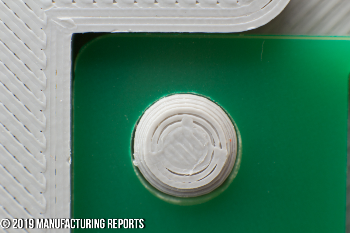
The quality of the milled features of the board were disappointing. This was the first of the PCBs I’ve reviewed that failed the mechanical jig test, which was so surprising I had to go back and verify all the measurements. Sure enough, the two boards that failed would never have fit into an product enclosure using the tolerances published.
The mechanical holes were almost universally over sized, and a rough edge finish left on a number of boards — there was a distinct rough finish as you passed your finger along the upper edge of those boards. Witness marks were visible on all PCB edges. Mechanical slots were all very large either just barely slipping under the tolerance limit or exceeding the allowance.
Trace widths were good overall, if undersized by a 1 or 2 mill here and htere, with only four individual traces exceeding the 80% under size tolerance.
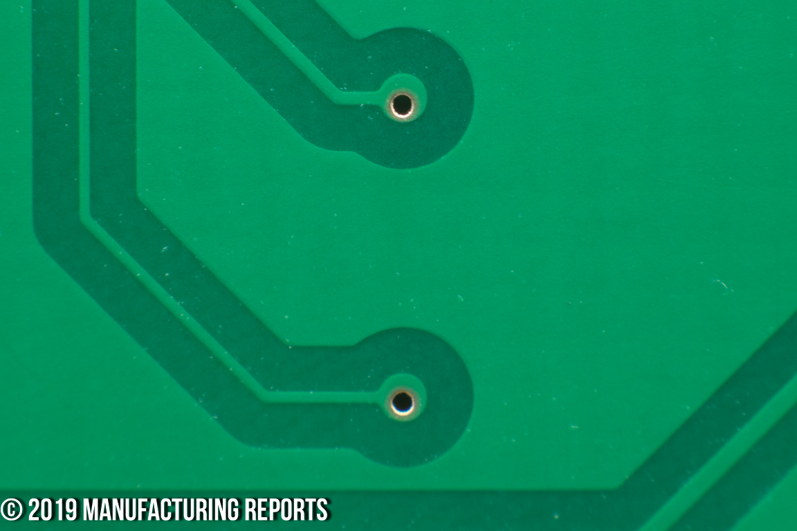
Vias were a mix of both excellent fabrication and a few really rough offsets. The plated slots were straight but not entirely perpendicular.
- Board Edge Quality
- Milled Feature Quality
- Dimensions – Edges / Slots
- Positioning NPTH / PTH
- USB Connector Slots Straight
- Trace Widths
- Via Centering
Smart Prototyping NOA Labs Test Report 2019
-
- Good Via Drills
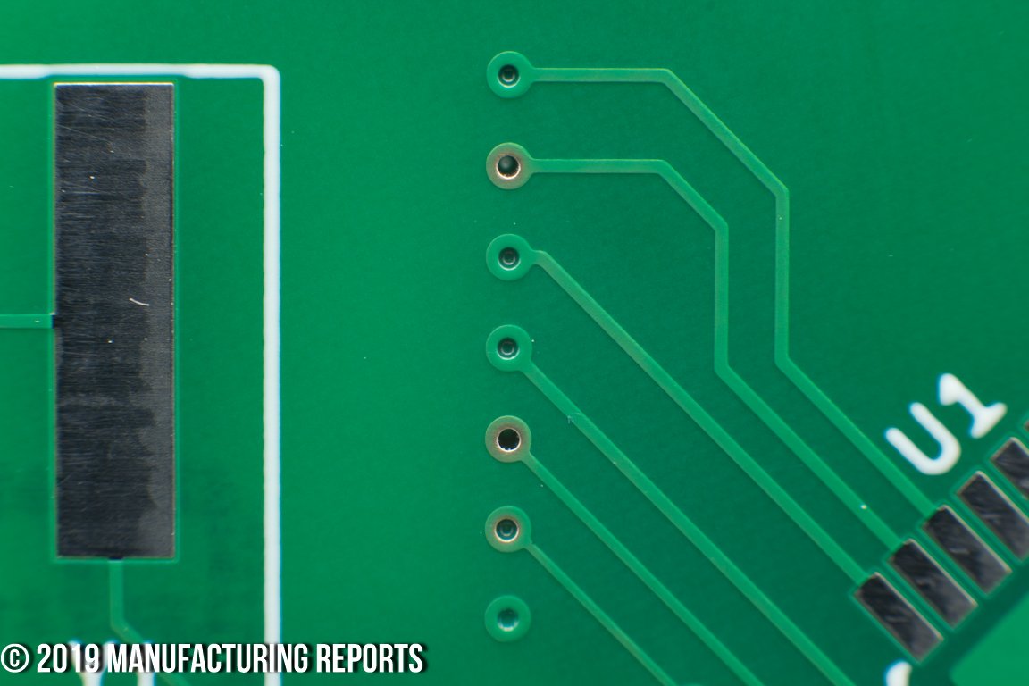
-
- Varied Via Drills Sizes on Center
-
- Bad Via Offset
-
- Plated Slots
-
- Saw Tooth Board Edge
-
- Board Edge Angled View
-
- Rough Mechanical Milling
-
- Witness Mark on Edge Cut
-
- Board Passing NPTH Position Test
-
- Board Failing NPTH Position Test
Copper Layer Quality
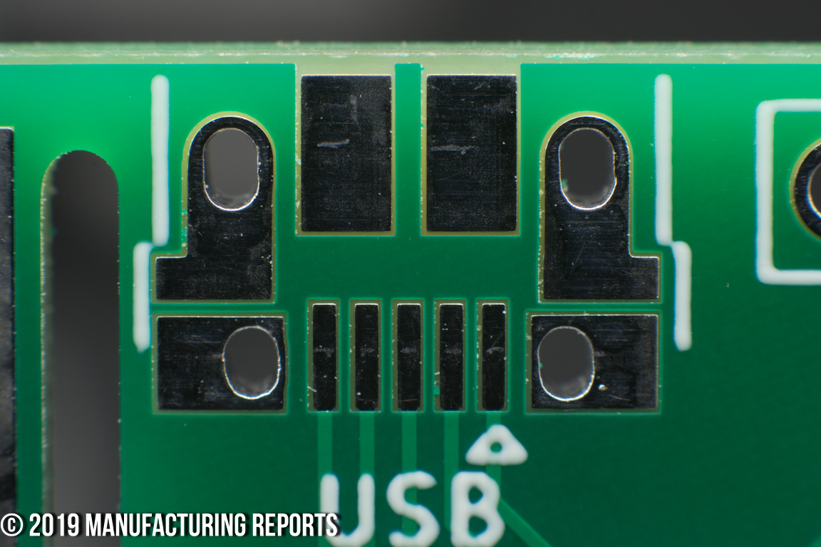
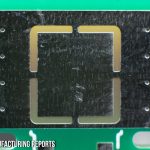
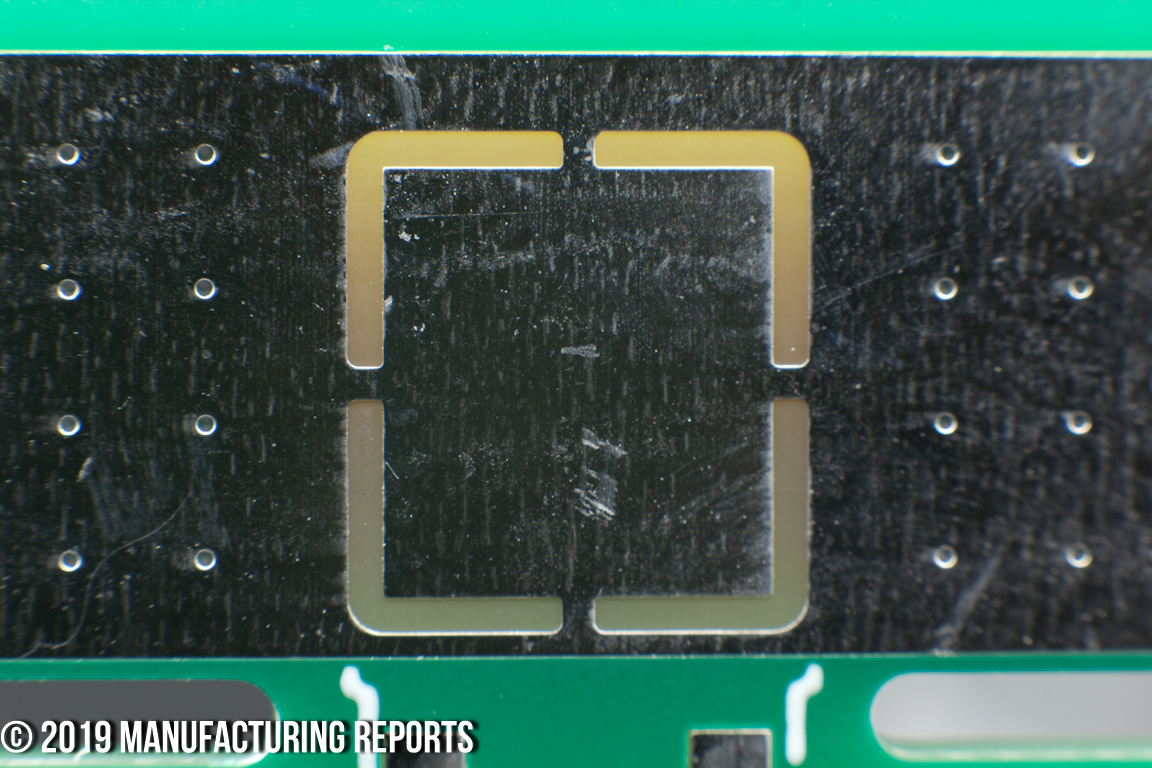
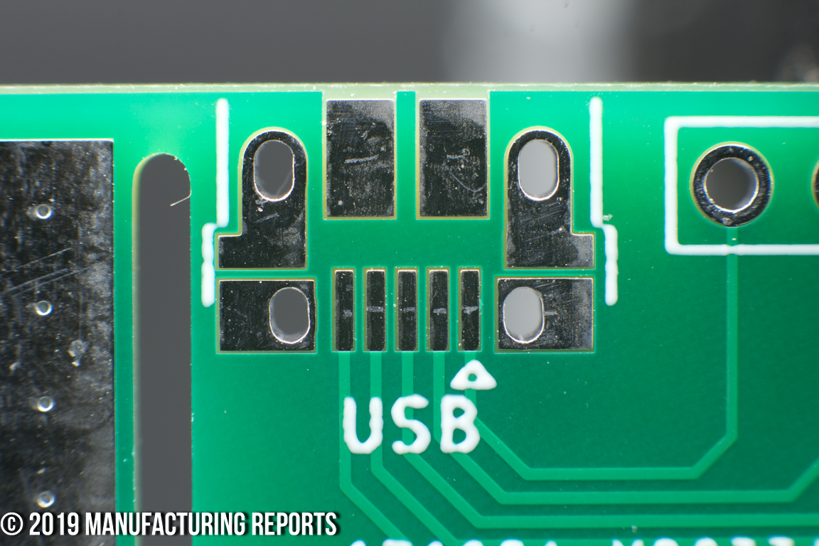
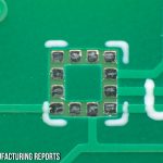
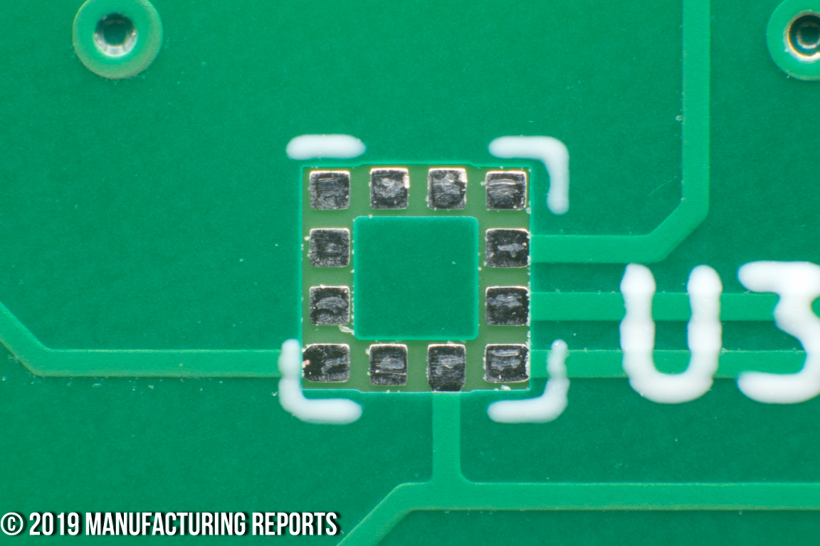
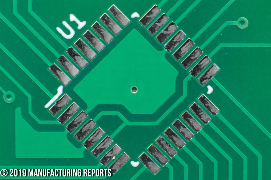
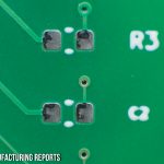
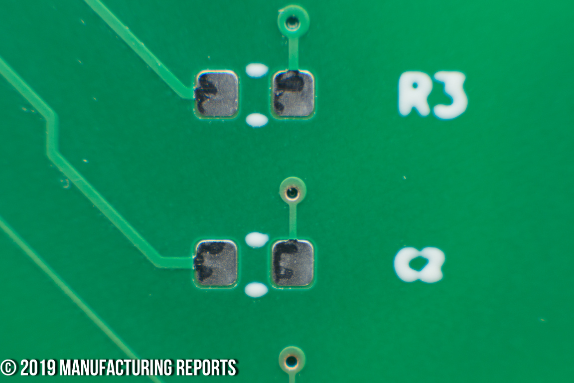
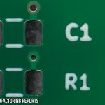
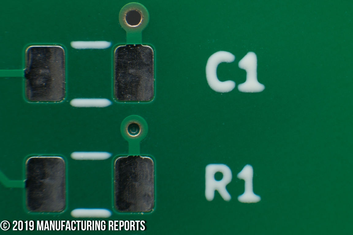
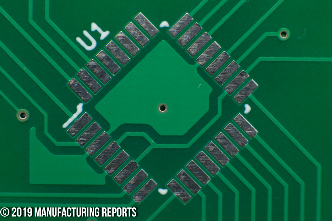
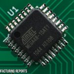
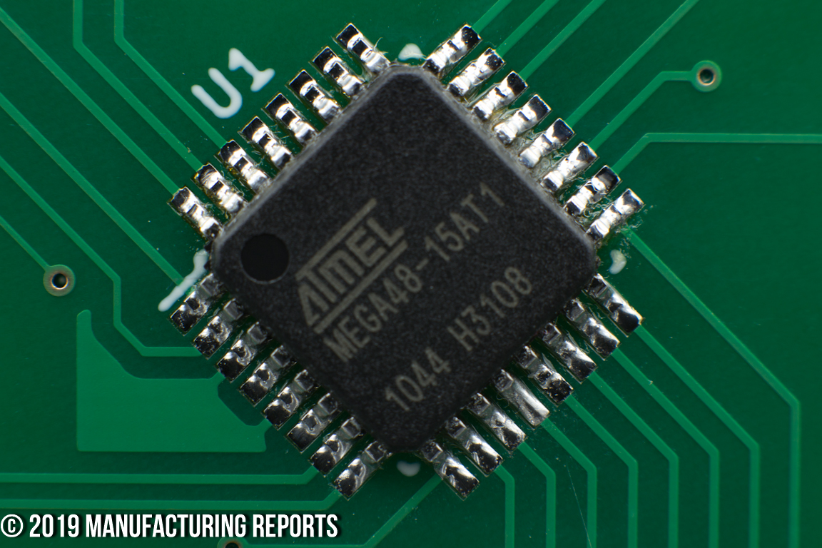
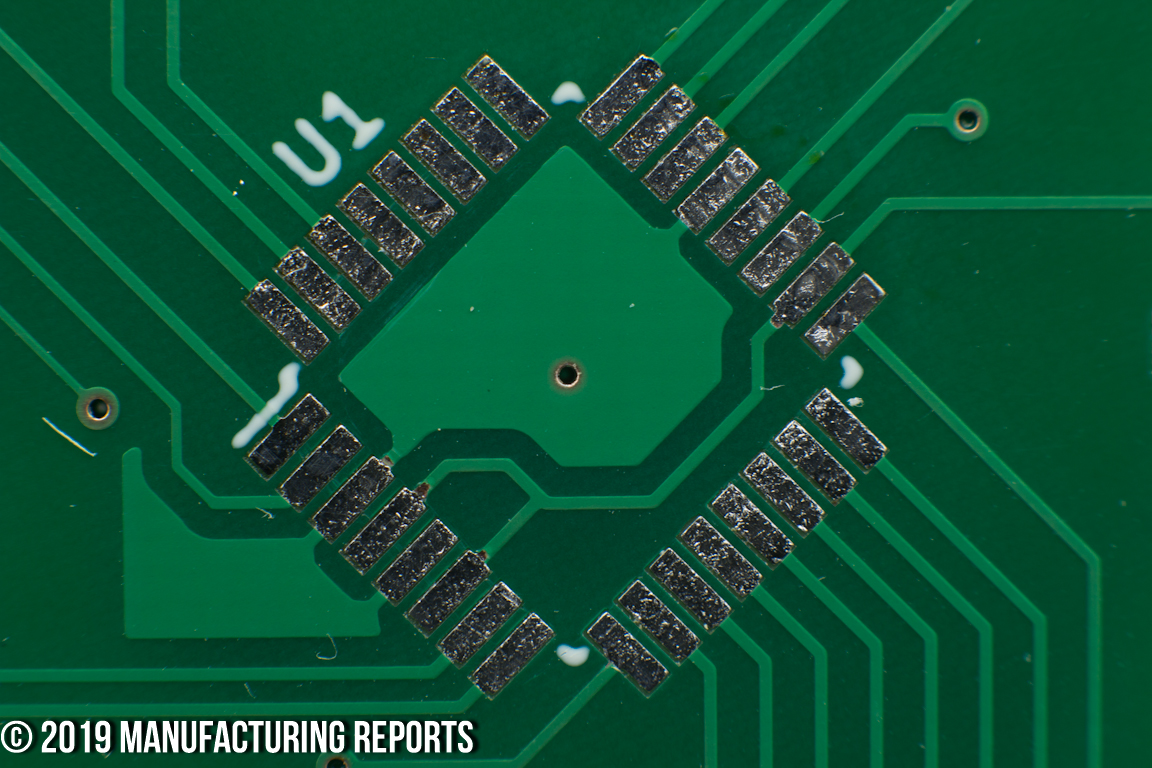
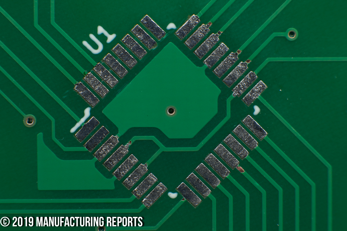
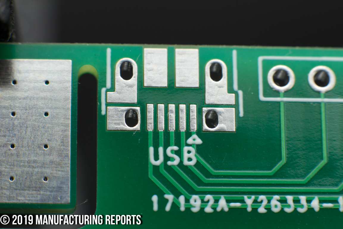
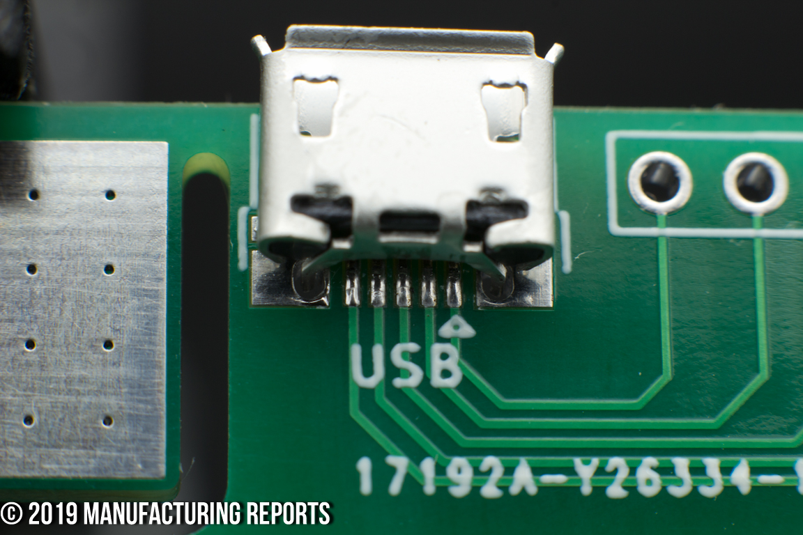
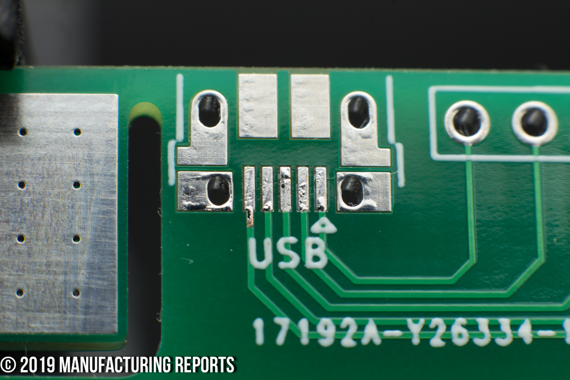
I’ve spent so much time looking at low cost prototyping boards that I’ve gotten to the point of being shocked to say that none of the vias or the traces on these boards were damaged. There are no scrapes, cuts or mutilations of the copper layer at all. The QFN and QFP footprints were well formed and correctly sized, as were the passives footprints down to the 0201. The USB connector was also correctly fabricated with the plated slot offset 0.25mm from the pad edge as per the design files.
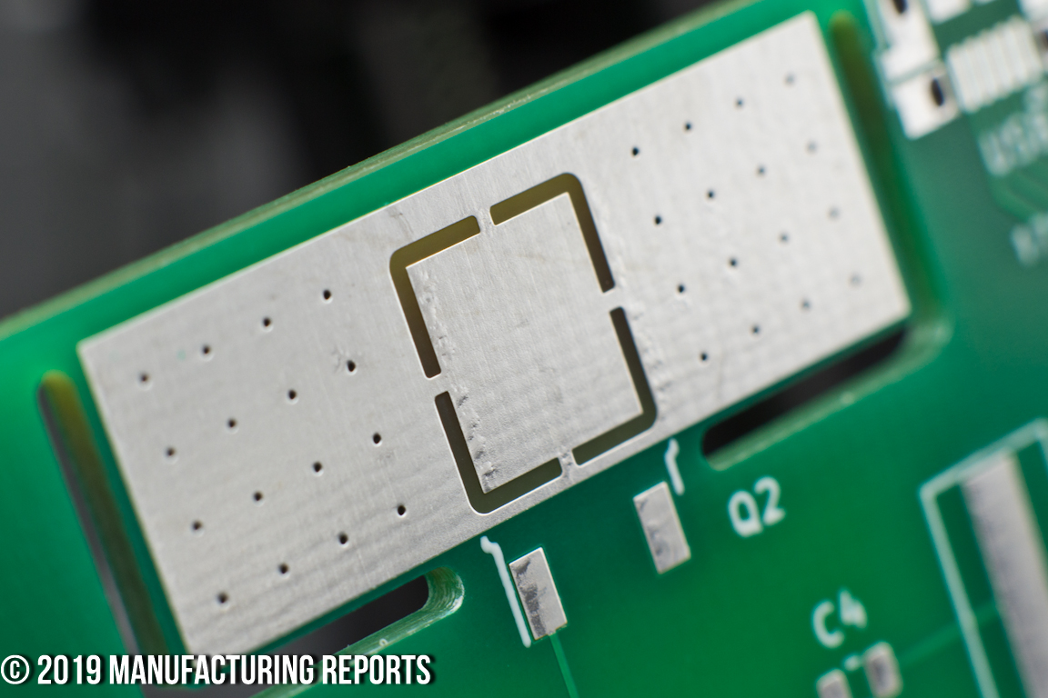
The HASL surface finish on these boards is perfectly average, with minor surface wrinkles and ripples, but not the worst, and the copper weight all measured within 1oz tolerance.
-
- Average HASL Surface Finish
-
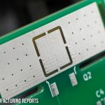
- HASL Over Heatsink
-
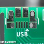
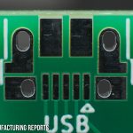
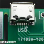
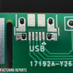
- Micro USB Footprint
-
- 0201 Footprint
-
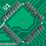
- QFN Footprint
-
- QFP Footprint
Solder Mask Quality
The solder resist layer is where many manufacturers suffer, allowing the boards to get scratched, scuffed and dinged to such an extent that no surface coating in the world would protect the underlying copper from damage. In the case of these boards, they are free of all that, with a few exceptions so minor that I just can’t get any correct angle of light on them to photograph. The footprint apertures are correctly sized and the registration of the solder mask layer is correct across all boards, preventing any overlay of solder mask onto pads. The mask ink didn’t appear to have wicked through any of the vias, including in the heatsink area.
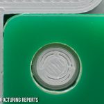
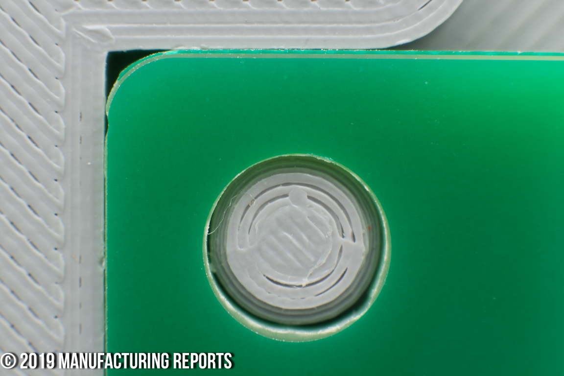
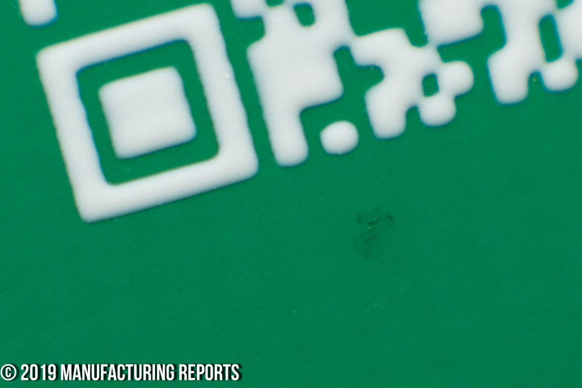
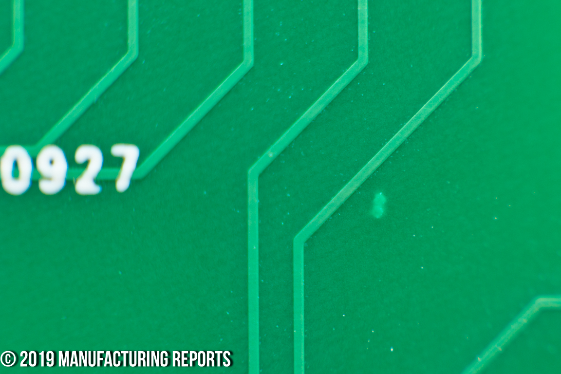
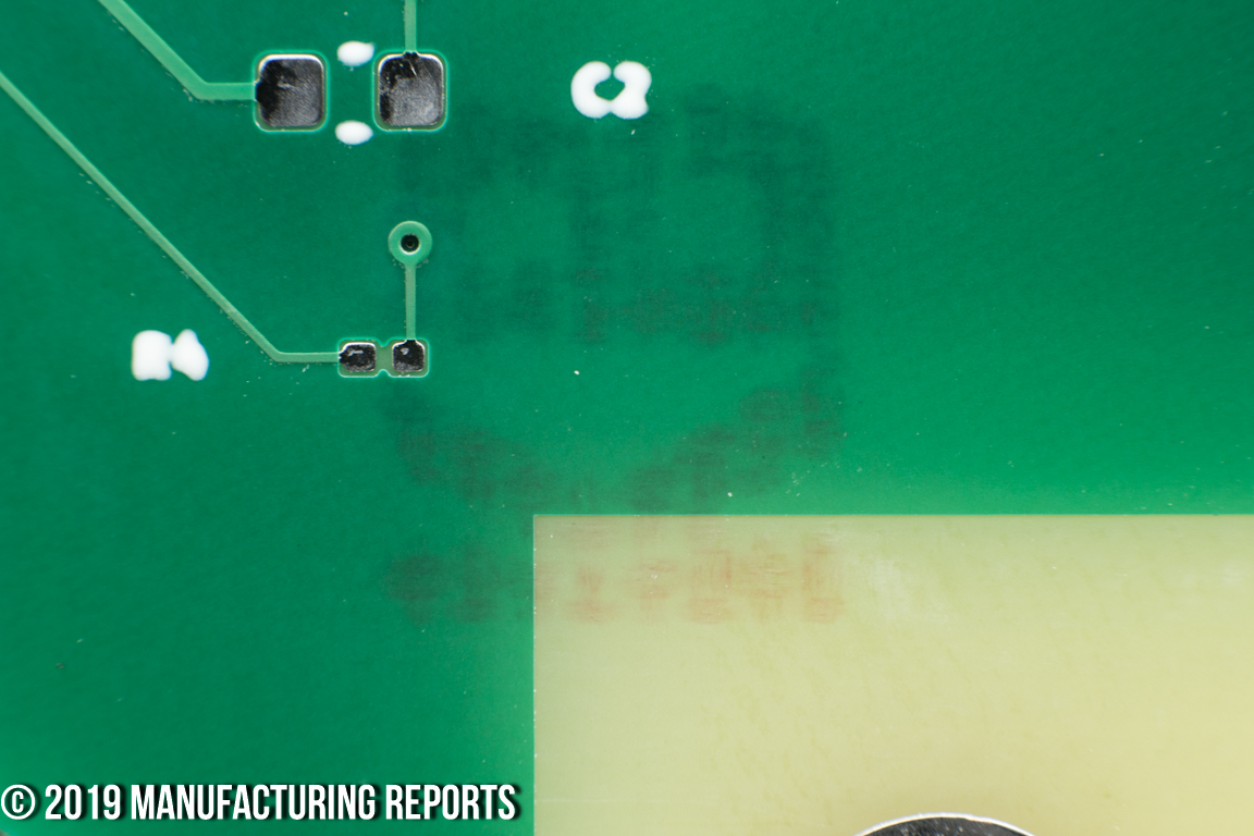
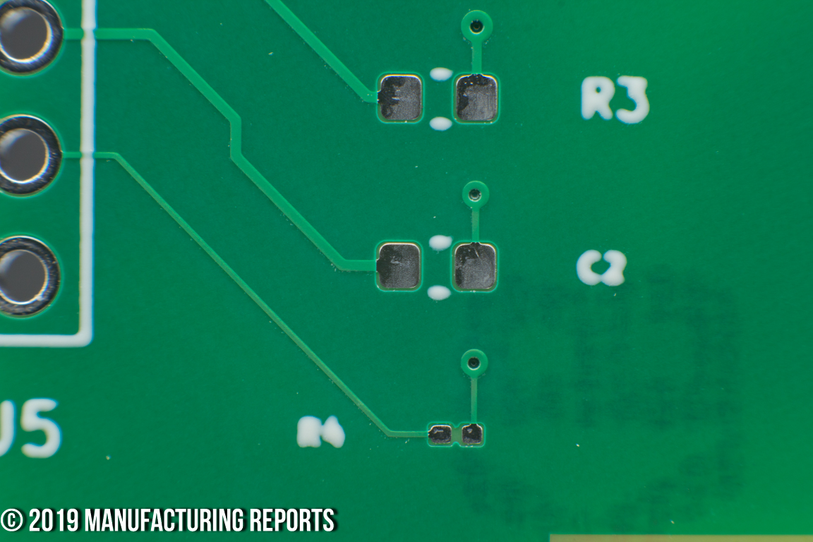
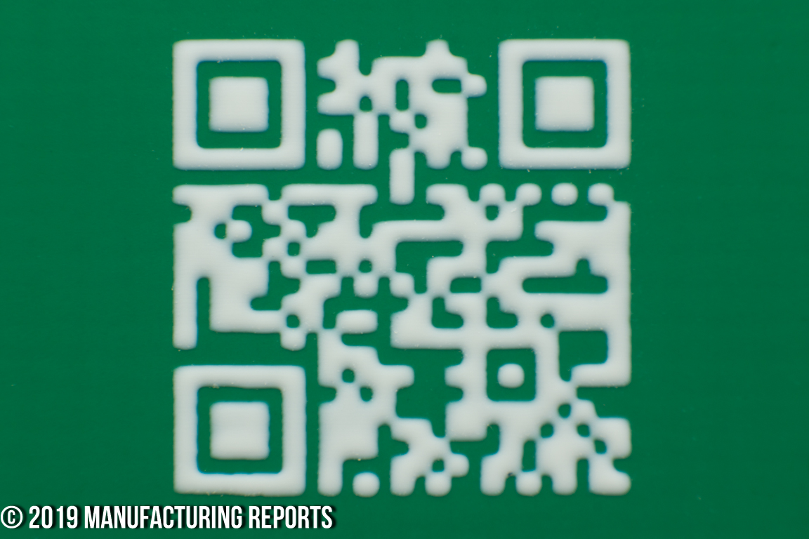
Unfortunately, the mask layers are visibly thin on each PCB, with many vias barely tented or free of mask entirely. Several boards also had contaminant spots in roughly the same upper-right-front location.
-
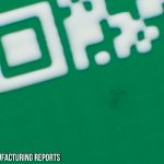
- Contaminant by QR Code
-
- Contaminant Under Mask
-
- Substrate Logo Visible Through Mask
-
- Inconsistent Via Tenting
-
- Thin Via Tenting
Silkscreen Quality
I’m not as impressed by the quality of the silkscreen on these boards as I was with the silk layer from ITEAD, even though, again, they seem to be from the same factory. Somehow I found the quality a bit more “blobby”. I still think this is direct legend printing, not LPI, but not of the same resolution as the other boards.
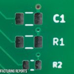
The resolution of the QR Code required some magnification to resolve, but eventually did, and the passives reference designators were legible down to the 0.75mm font height, but C2 and R4 were messy and ill-defined below that. Text over traces was rendered well despite the varying z-height of the surface.
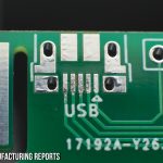
There were no blemishes, misprints or overprints, however a manufacturer’s mark was printed prominently below the USB Connector.
-
- Font Below 0.75mm Illegible
-
- 1mm Font Height
-
- 2mm Font Size
-
- QR Code
-
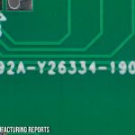
- Manufacturer’s Mark
Solderability
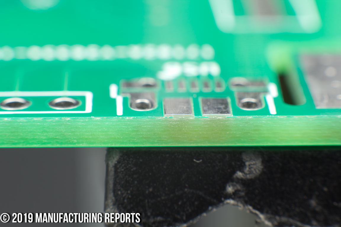
A PCB was selected at random and subjected to soldering tests. Both the QFP32 and USB Micro Connector components were easy to solder down, sitting flat on their pads during the process.
The QFP 32 showed nearly no degredation of the solder mask layer after the first rework, with minor nicks removed from the traces of a few pads. Even after the second rework, the footprint looked in much better shape than other manufacturers boards have looked after the first round. The solder mask, though thin, does appear to show good resiliency to the process of soldering / cleaning / reworking the part off / cleaning and resoldering.
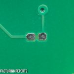
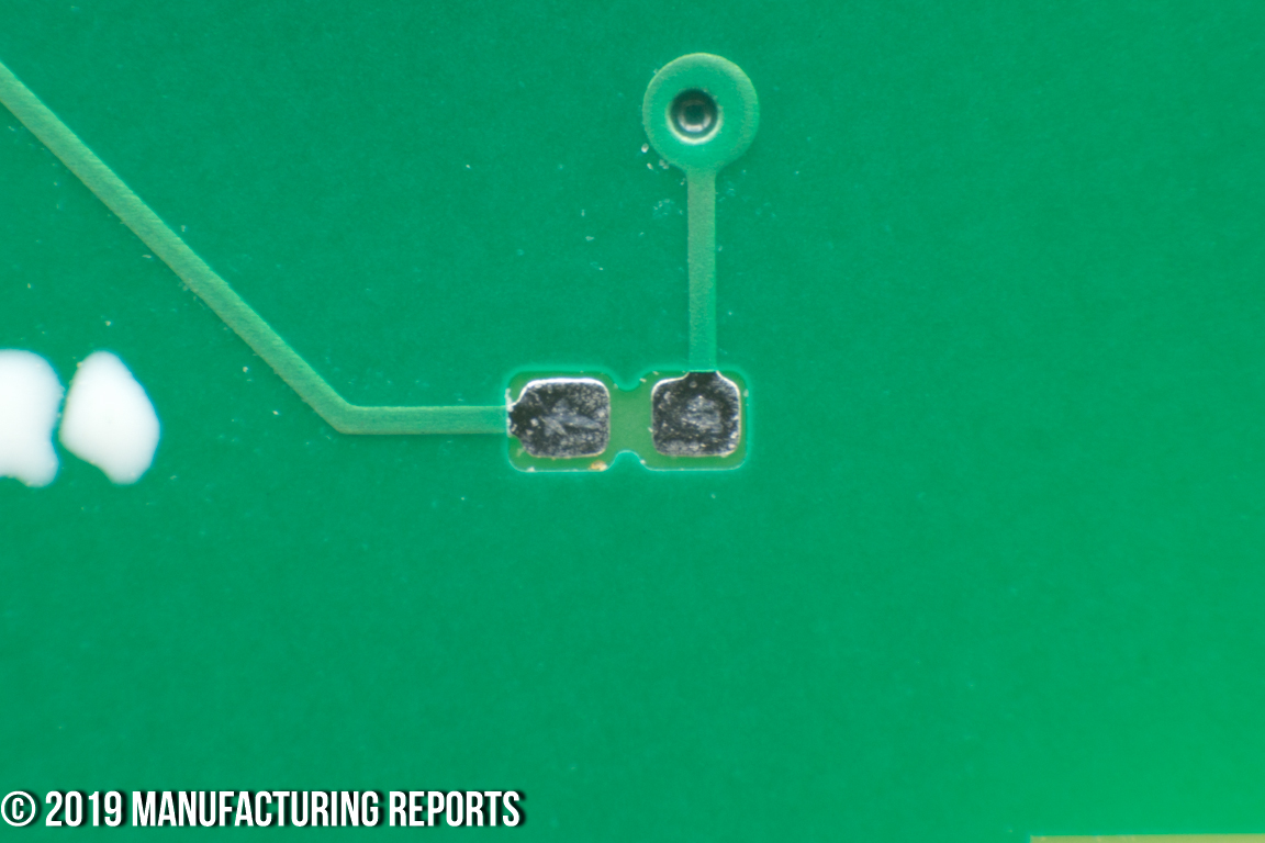
The USB Micro demonstrated similar resiliency to mask erosion after the first rework, with only a slight increase in the pad length occurring to one of the footprint lands. After the second round, the trace erosion increased slightly, but the mask web between the pads also started to suffer, with over half missing between pads 2 and 3, and the beginning of erosion occuring between 3 and 4.
The silk screen was unaffected at either footprint by the rework processes.
-
- QFP32 Before Soldering
-
- QFP32 After Soldering
-
- QFP32 After First Rework
-
- QFP32 After Second Rework
-
- Micro USB Before Soldering
-
- USB Micro After Soldering
-
- USB Micro After First Rework
-
- USB Micro After Second Rework