ITEAD Prototype PCB Review

ITEAD Intelligent Systems Co., LTD
Shenzhen, China
$1.49
Unknown
MRTC v2.1
Excellent Silk Layer
Mask Relief Around SMD Pads Spot On
Plated Slots Really Well Fabricated
Excellent Resiliency to Rework
Messy Ordering System
Lack of Clarity on Turn Time
Poor Quality Milled Features
Via Tenting Lacks Consistency
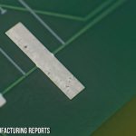
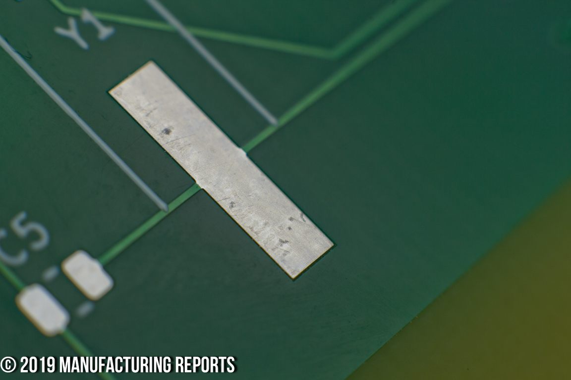
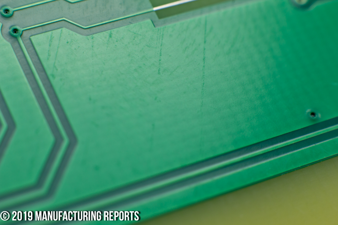
Surface Scratches
ITEAD Intelligent Systems Co., LTD, also called Sonoff, is a Shenzhen based PCB fabricator and PCBA service provider. As is usual, they offer not only fabrication and assembly services, but also host a market place, the “IMALL” for boards sourced inexpensively in China or designed in-house. They also have a blog with over 450 posts dating back to 2010 that used to contain articles about things like hacking a Saleae Logic Analyzer but now is mostly about smart homes, IoT and stock photos.
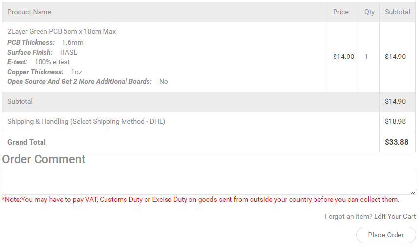
Cost
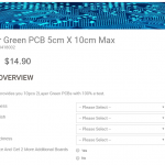
The purchase price for whatever it was I purchased (as of the writing of this section, I still haven’t received confirmation that the order was for 1 or 10 boards), was $14.90 with an additional $18.98 in DHL express shipping from Shenzhen.
Dan of Two Weeks Later can confirm that 10 boards were delivered, even if it was never confirmed during the ordering process.
Ordering
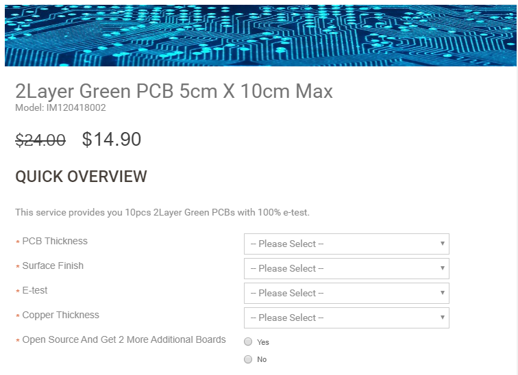
Finding how to place an order was a little tricky at first, as you had to put a “2Layer Green PCB 5cm x 10cm Max” in your shopping cart, at which point a very rudimentary stackup page was loaded, allowing you to select PCB Thickness, Surface Finish, Copper Thickness, and E-testing.
A weird item was presented as well, “Open Source and Get 2 More Additional Boards”, which is a strange thing to ask at time of ordering. Considering that none of the items for sale in their IMALL seemed to be released under any kind of open source hardware license (their wiki does have schematics for some of the products), and with zero links or descriptions as to what you’re giving up or agreeing to by selecting that, I thought it wise to leave it set to “No.”
It is also confusing that no where does it explicitly state the quantity of boards you’re ordering. Navigating various pathways through their purchasing system, I developed an assumption that the “2Layer Green PCB 4cm x 10cm Max” product I’d added was a 10 board order, so the quantity I placed in my shopping cart was “1”, and hoped for the best. (10 boards were delivered)
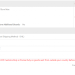
Checkout is performed prior to uploading Gerbers. I was given the option of checking out as Guest, but based on previous experience I’m just avoiding that from now on: having an account with a dedicated account page just makes it easier to track order status. During the payment process I was warned about VAT, Customs Duty or Excise Duty several times, which no other manufacturers have done, so I suppose I became a little worried that the tax man would knock instead of DHL once the boards arrived. (Ultimately, this seems to have been a non-issue — the boards arrived as usual.)
No email was received to confirm the order after submitting payment. I went to my ITEAD account page and the order status was “File Uploading”, but no readily apparent link visible to actually provide Gerbers. If I was new to ordering boards, I wouldn’t even necessarily know there was an extra step necessary at this point, and no information is presented to direct you to give them the files. I did discover an upload link in the “View Order” section of the order status, with angry red letters saying “This is the QTY of PCB service consumed by the Gerber file you upload.”
Clicking the upload button brought me to a page that suggested a Gerber preview was possible, but that they had “failed to analyze your gerber file, but we’ll review it manually. Everything is fine.”
No estimation of ship date was provided.
-
- Ordering Options
-
- Customs Warning
Fulfillment
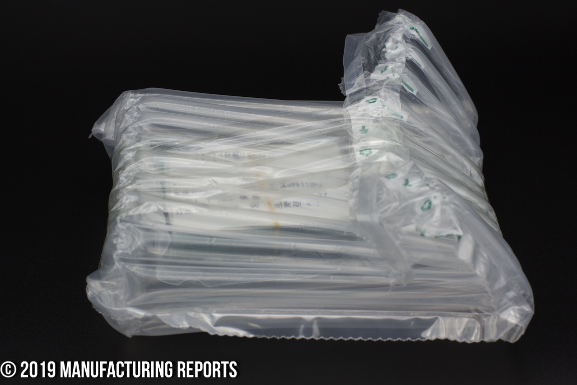
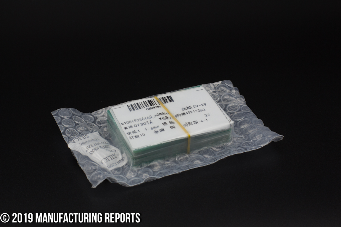
Fulfillment was excellent. The order shipped far earlier than I expected, in fact, they hit their regular ship date despite customer service letting me know the order would be delayed by the oncoming Chinese “Golden Week” factory shutdown. When the boards arrived in their DHL vinyl pack, they were secured in a thick bubble sausage pack, and then inside of that was the standard vacuum bubble wrap, with a little sachet of desiccant. From a fulfillment perspective, that’s quite a bit of financial outlay above what others are doing. Full marks to ITEAD for that.
-
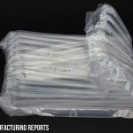
- Outer Bubble Sausage Pack
-
- Inner Vacuum Bubble Pouch
Customer Service
Feeling very in the dark after submitting the gerber files, I looked for a way to contact ITEAD. On their Contact Us page, was a “Help & Support” form I filled out asking for the expected turn time, confirmation that I would be receiving 10 boards and confirmation that the gerbers were uploaded correctly. While no order confirmation has been received yet, at least I did receive confirmation that they had opened a ticket.
The next morning, I received a response from an individual with the remarkable name of “Flame” (however, not “Rage Flame” the Deformation Robot, unfortunately) saying that the order would be fulfilled after the Chinese Golden Week holiday.
Design Rules were very difficult to find, with the link buried on the Support page under “Normal Condition of PCB capabilities.” “Requirements on the PCB Design” only explains what the outer board dimensions are and explains the concept of vias and minimum silkscreen line widths.
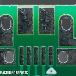
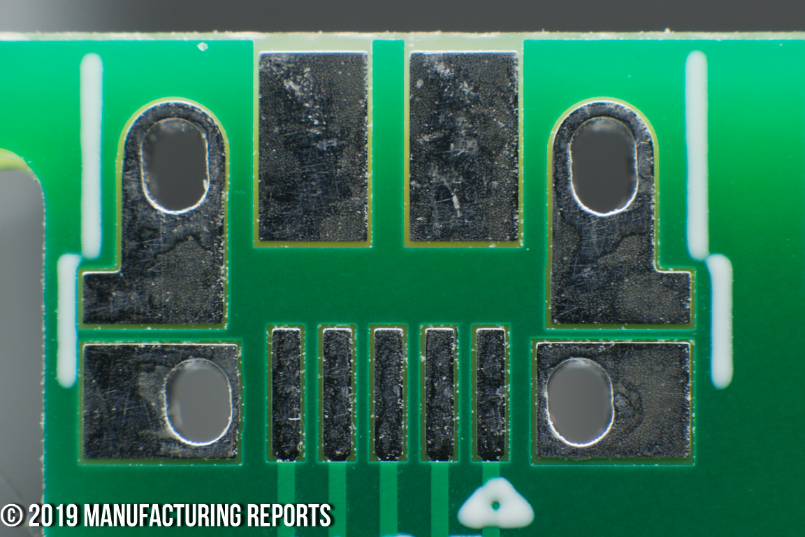
Circuit Board Visual Inspection
-
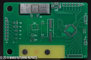
- ITEAD Review Full Board Front
-

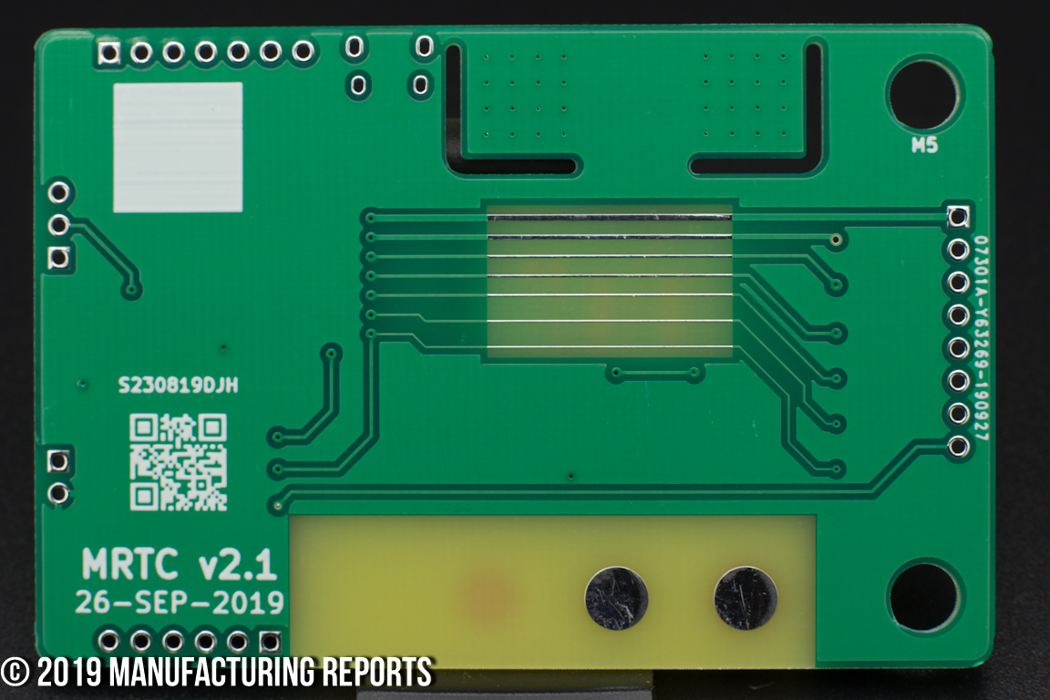
- ITEAD Review Full Board Back
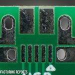
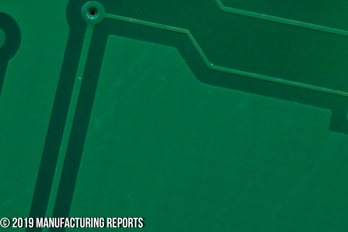
The boards were incredibly consistent, both in the quality of their copper and the haphazard nature of their milled features. The footprints and exposed copper features looked beautiful and clean on these boards, with only occasional thin application of solder mask over tented vias being the most significant issue. There are the usual scuffs and scrapes, with some significant amount on only one of the boards, but none that exposed copper or appeared to deteriorate the resist layer.
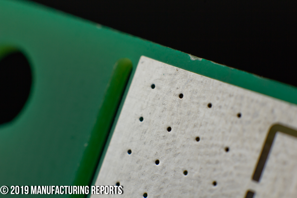
The milled features are sloppy though. My suspicion is a lack of rigid work holding combined with poor chip evacuation resulting in imprecise features and some minor delamination of the substrate.
PCB Dimensions
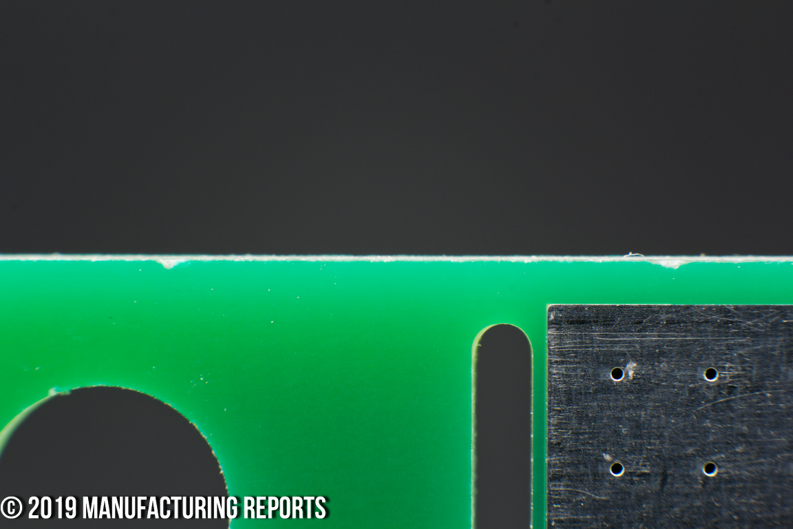
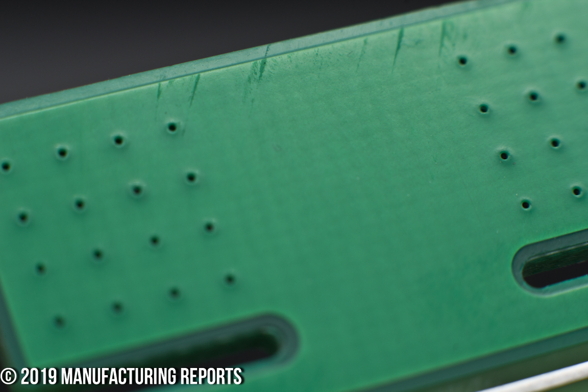
The board edges are all within tolerance, although barely in several cases. Further, the edges of some of the boards are particularly rough, where I believe the amount of swarf generated by the milling process wasn’t sufficiently cleared out, resulting in the upper layer of the FR-4 fiberglass layer and the solder mask being chewed slightly.
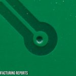
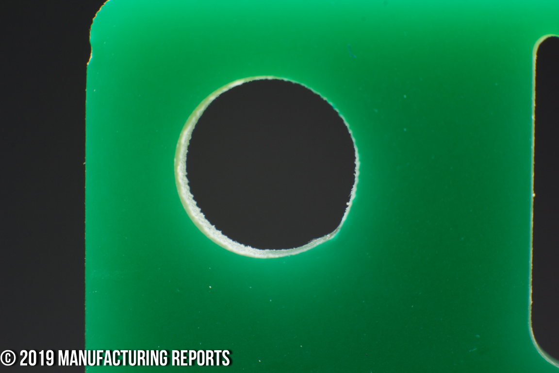
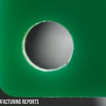
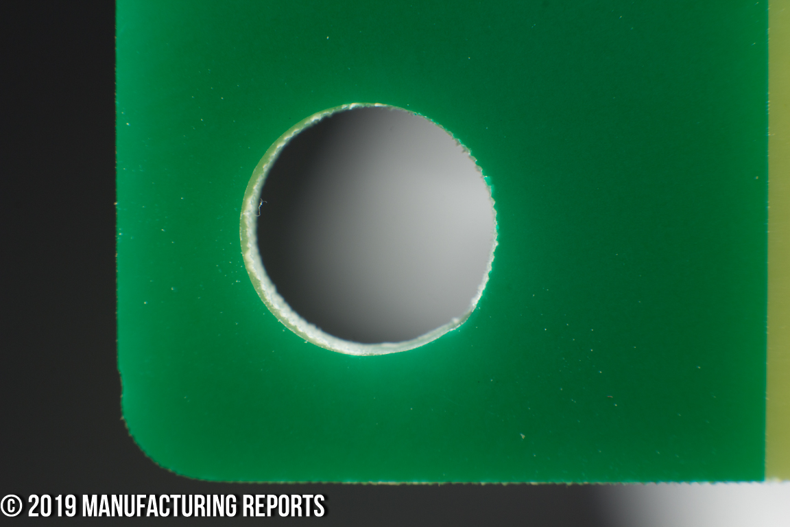
Most of the boards had both milled holes out of tolerance and out of round, due to significant lead-in / lead-out marks. I also noted some minor delamination of the substrate in those areas as well.
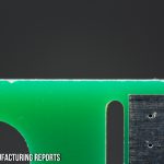
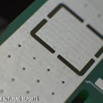
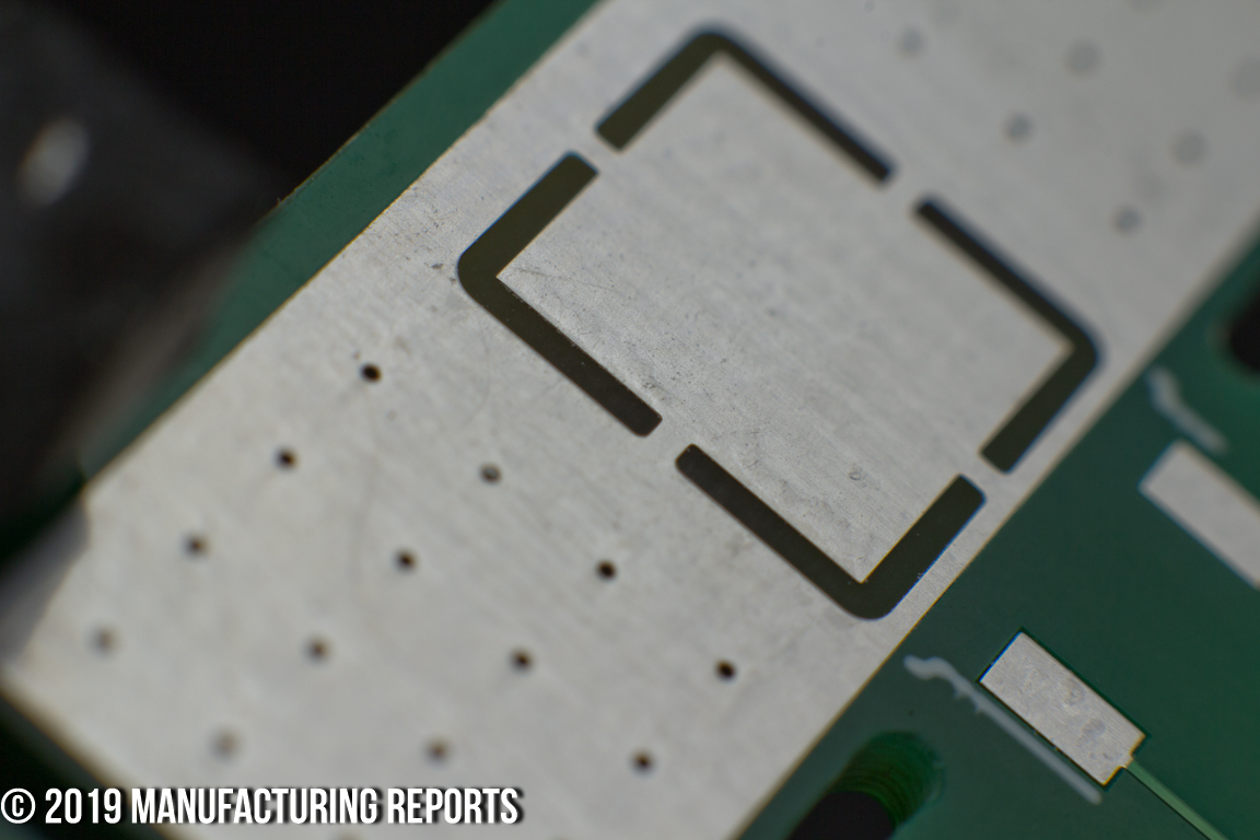
The mechanical slots were universally over-sized by at least 0.1mm and in three cases going over tolerance. The plated slots were excellently formed, clean and well positioned within their footprint pads, but slightly off from direct vertical.
The trace widths were good if slightly undersized on a consistent basis, with only 3% of the traces out of tolerance.
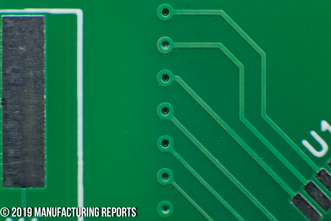
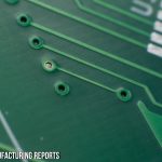
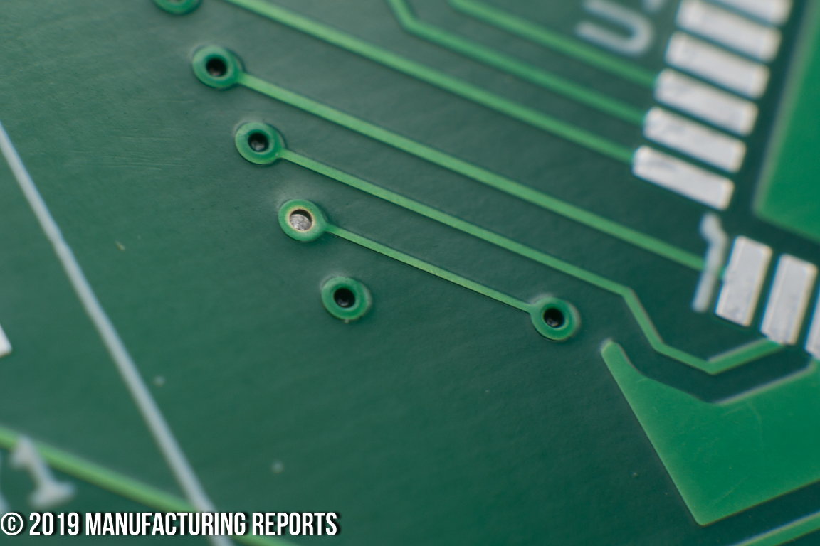
The via drills were some of the most precise I’ve seen in the low cost manufacturing space, with very few being more than marginally off center.
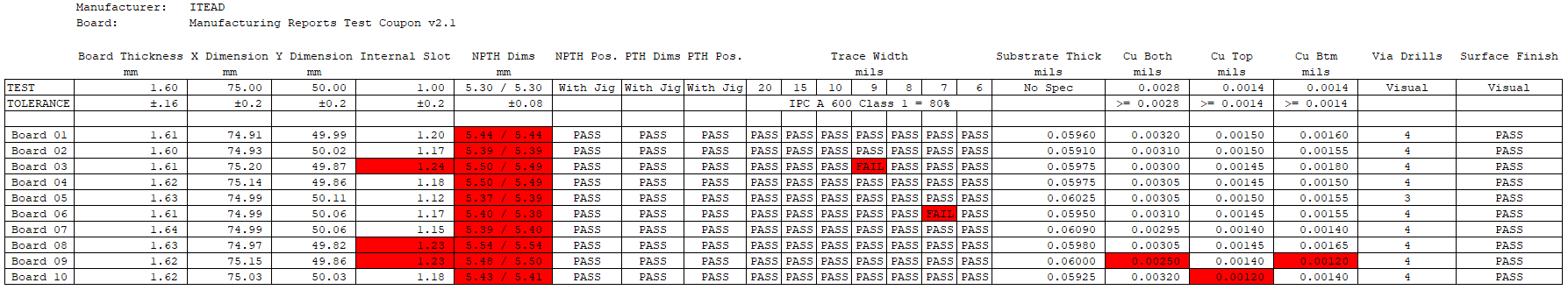
ITEAD Sonoff Test Report 2019
-
- Nicely Formed Plated Slots
-
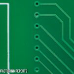
- Very Clean Via Drills
-
- Varying Sized Via Drills
-
- 0.3mm Drill / 0.6mm Ring
-
- Largest Offset I Could Find
-
- Slight Delamination
-
- Slightly Chewed Board Edge
-

- Edge Cut Witness Mark
-
- Large Witness Mark in Mechanical
-
- Roughly Milled Mechanical
Copper Layer Quality
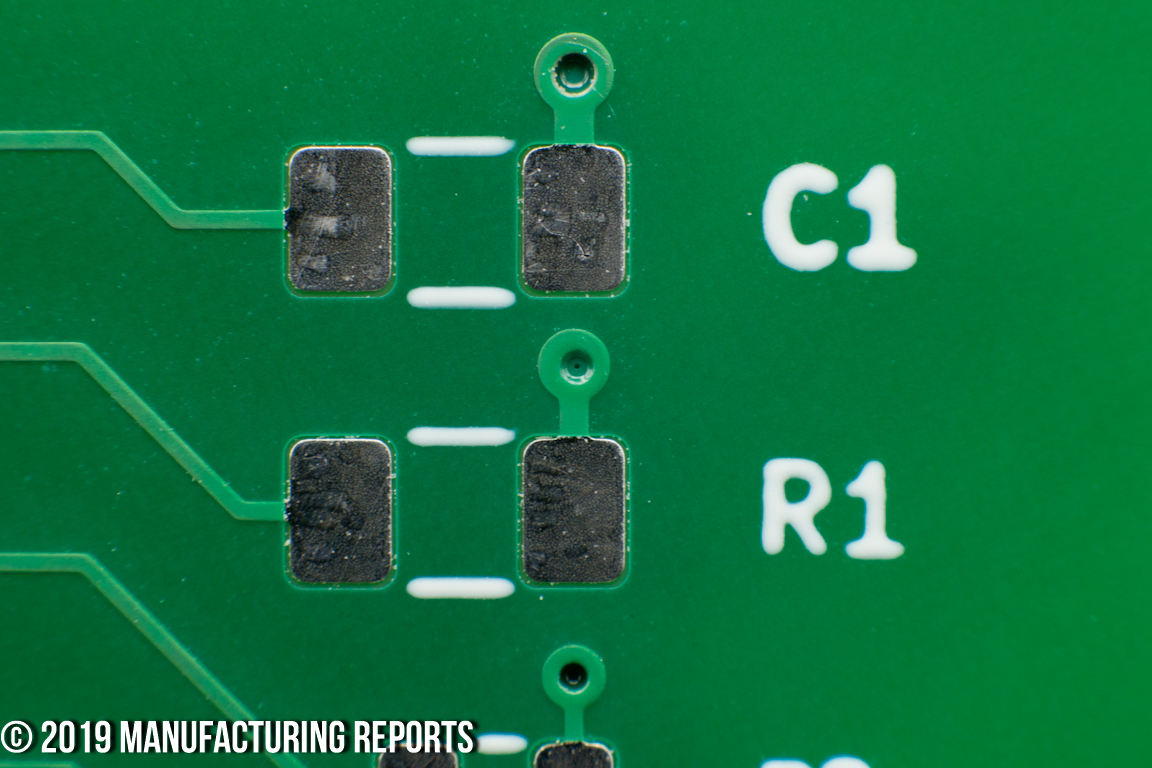
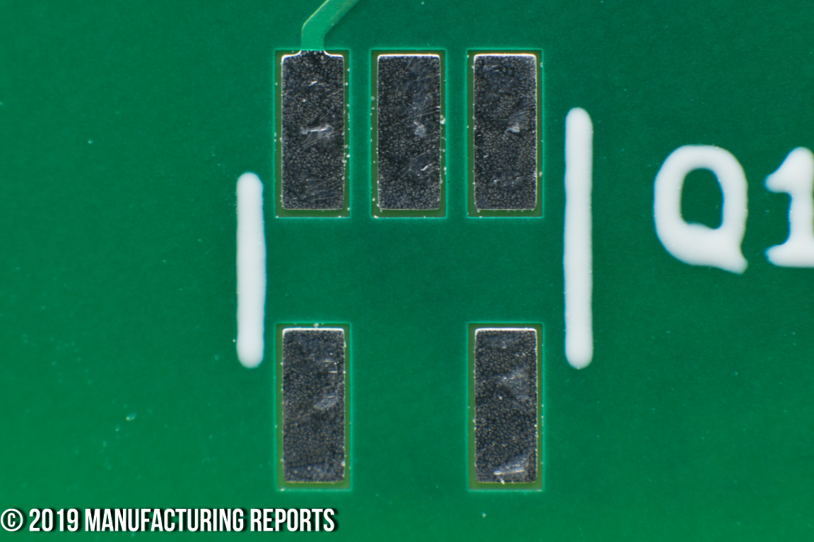
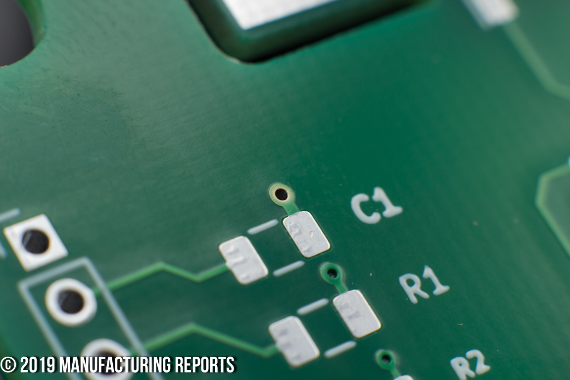
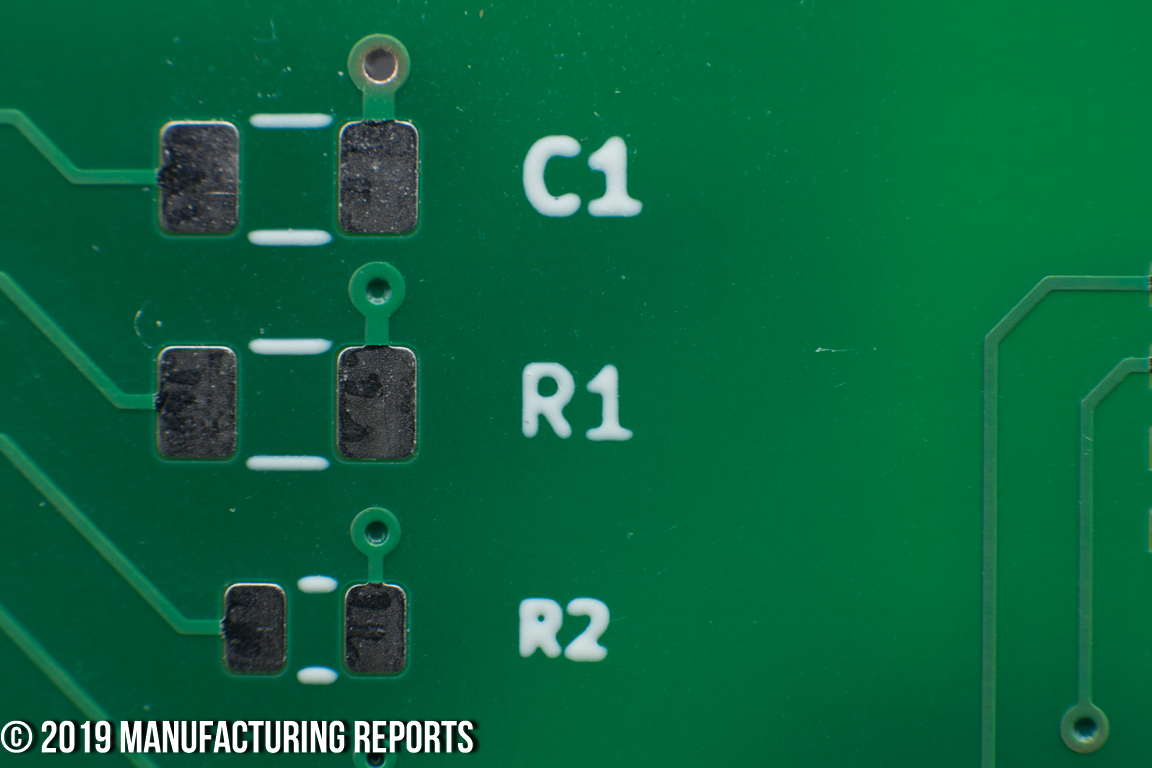
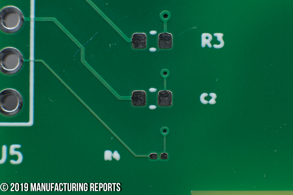
I was pleased with the quality of the ITEAD PCB copper overall. The HASL surface finish is well applied, but ever-so-slightly rough compared to the uniformity you see from some manufacturers. I find those slight deviations to be entirely cosmetic. The weight of copper is good except for one top layer and one bottom layer, both coming in .0002″ under tolerance. While there are some scuffs and scrapes on the boards, the traces and vias aren’t damaged.
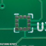
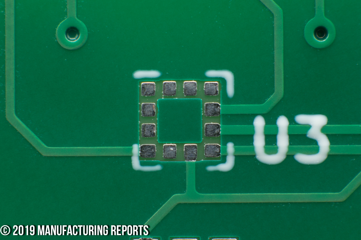
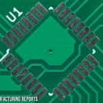
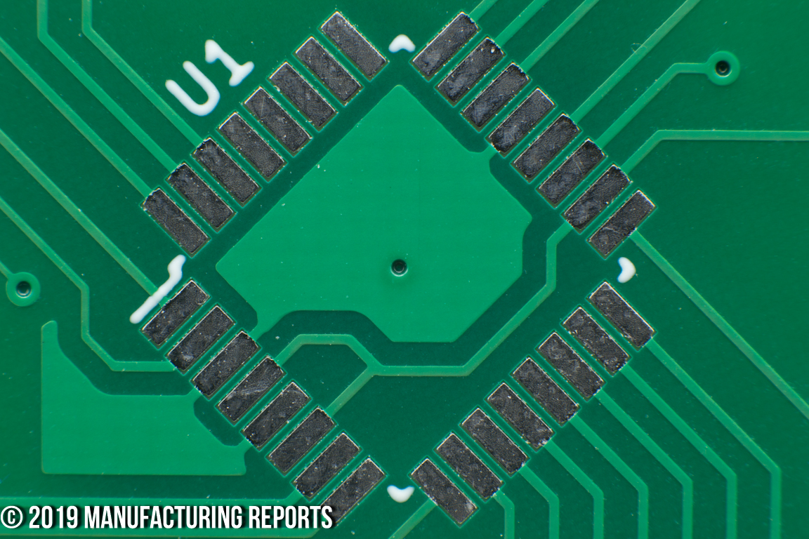
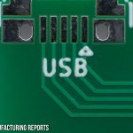
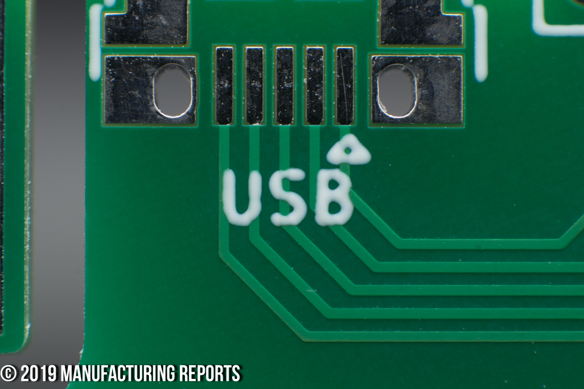
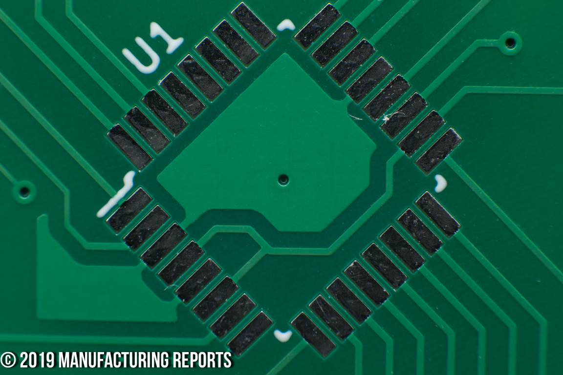
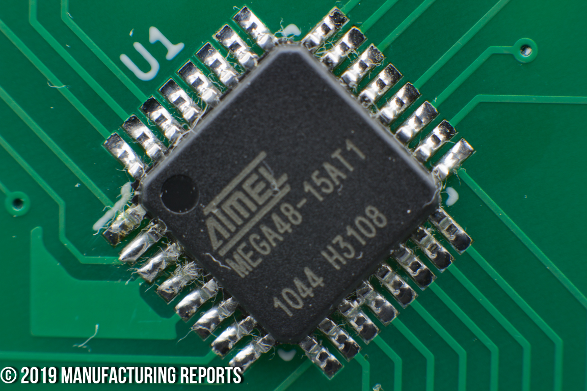
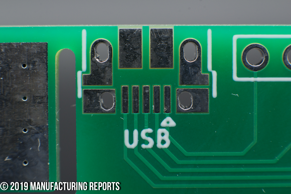
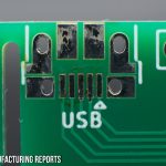
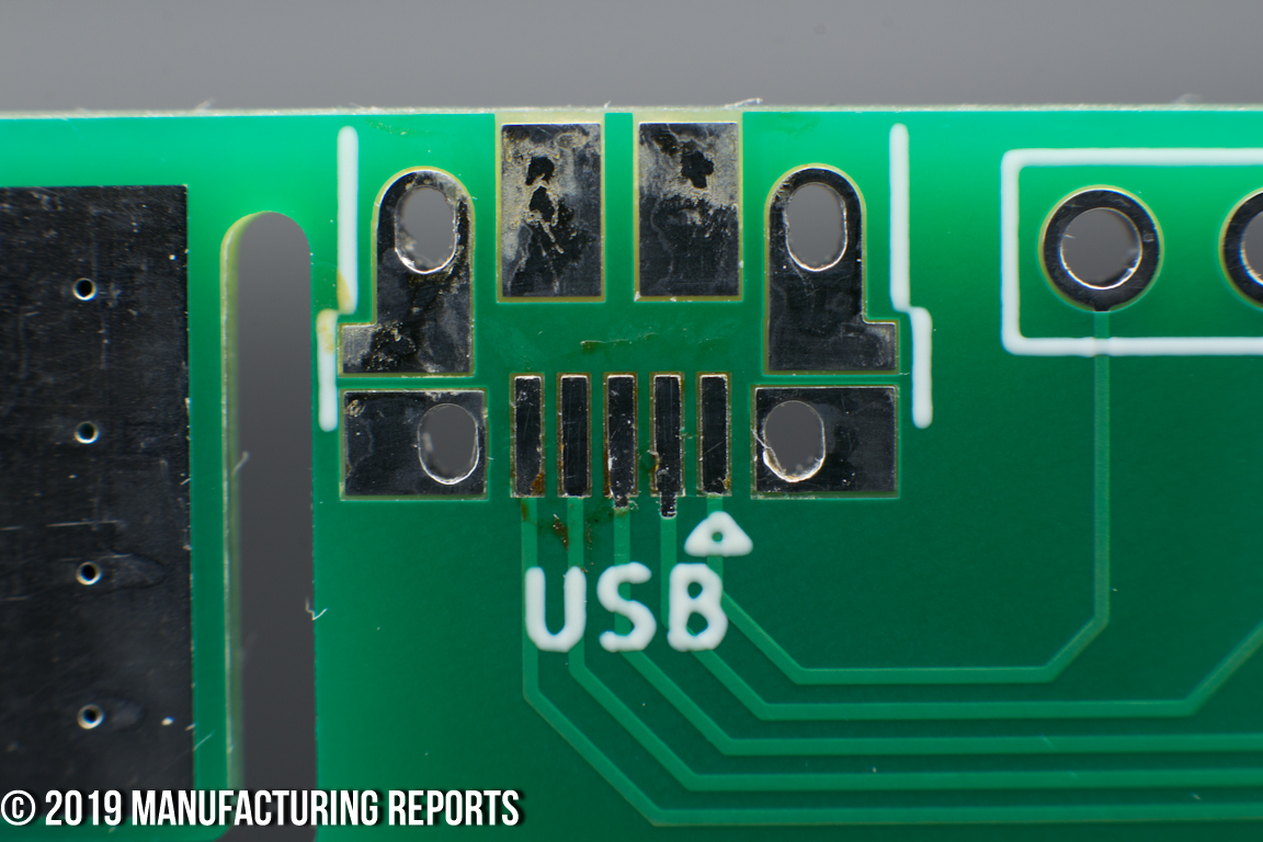
Footprints are well fabricated from the large crystal footprint down to the QFN and QFP. All passives footprints are intact down to the 0201, with even the smallest having sharply defined features. The USB connector has crisp pad definition. The plated slots, occasionally varying from directly perpendicular to the board edge, have straight sides and none of the “potato” shape you see on other boards. The offset of the slot from the pad edge is also correct at 0.25mm.
-
- HASL Surface Roughness
-
- HASL on Heat Sink Pad
-
- QFN Footprint
-
- QFP Footprint
-
- USB Connector and Plated Slots
-
- QFN Footprint
-
- Surface Scratches
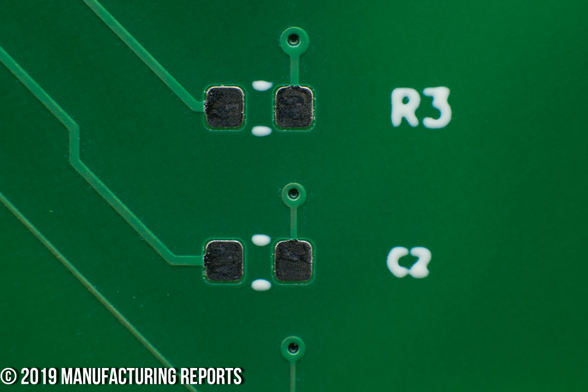
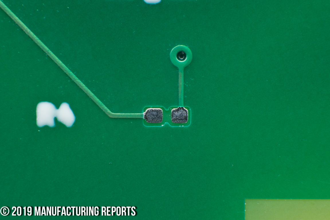
Solder Mask Quality
Overall the resist layer is of good quality, but thin over quite a few of the vias which should have been tented, and subsequently became clogged with solder during the surface finish application. In each case where I suspected the solder mask was thin enough to allow exposure of the annular ring, it toned out conductive to a pad on that via’s net.
The positioning across all boards was well within the 4mil tolerance and no pads had solder mask overlaying their edges. The back side copper pour isn’t exposed at the keep out area around the thickness testing pads of the MRTC.
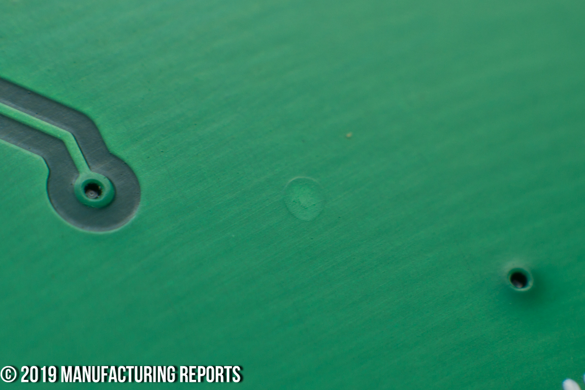
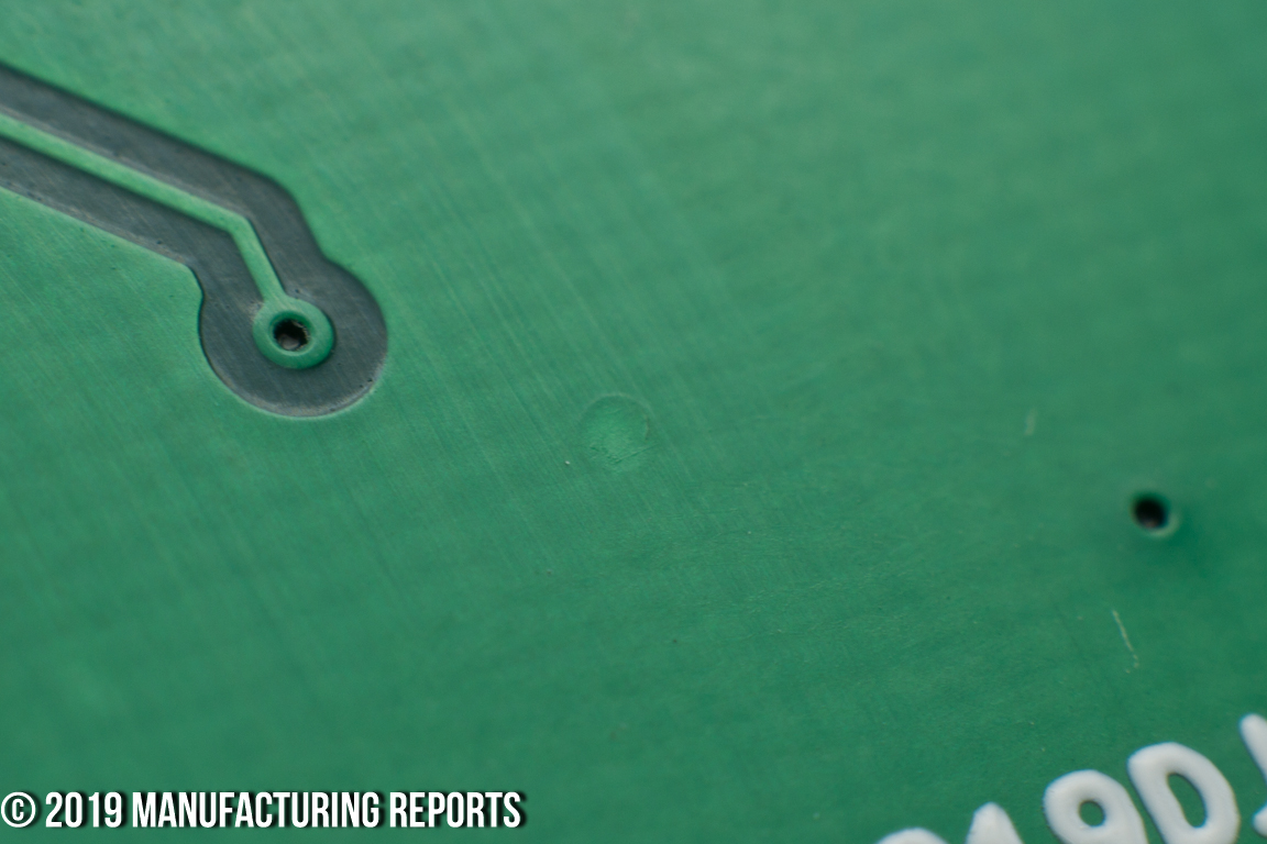
Looking at the surface quality and texture, two boards had some kind of contaminant, as though a drop of solvent had been left to dry in a particular location, but it was in exactly the same place on two boards which feels inexplicable. And while all the boards had some amount of light scuffing from shipping and handling, one board had a large scuff across the majority of the back side mask, however it didn’t penetrate to the underlying copper at any point.
-
- Excellent Mask Relief Around SOT23-5
-
- Mask Scratches Top
-
- Mask Scratches Mid-Board
-
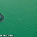
- First Contaminant Droplet
-
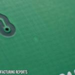
- Second Contaminant Droplet
-
- Via Clogged with Solder
-
- Thin Mask Over Via
Silkscreen Quality
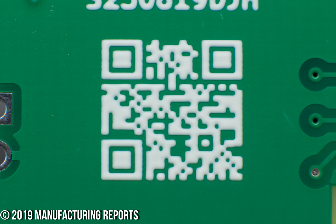
At first (second, eighth, fourteenth) glance, you could be mistaken for thinking the quality of the silk layer was created through a liquid photo-imageable process, but after looking again and again and again, the slight striation in the label area leads me to think that a direct legend printing method was used. If so, it is, by far, the highest quality DLP silk layer I’ve run across.
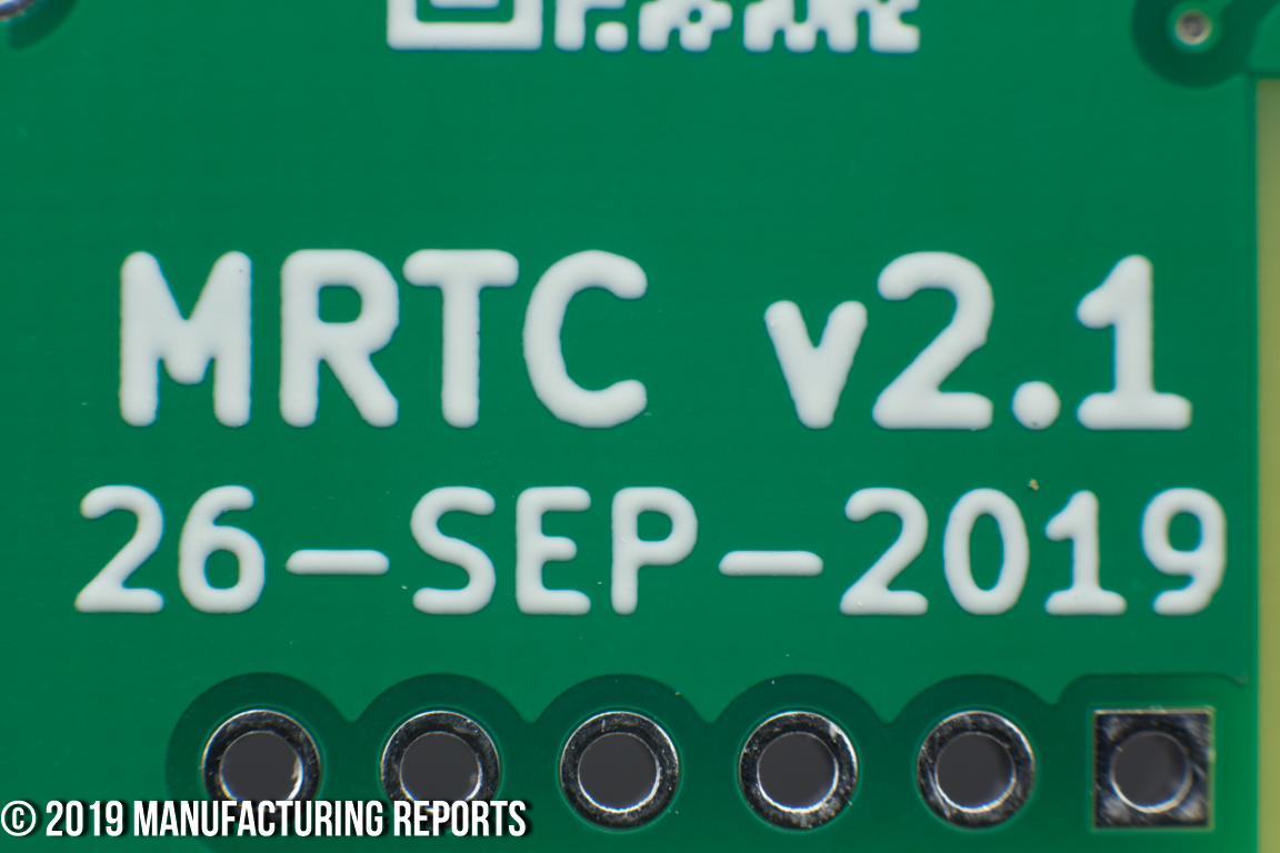
The ITEAD Design Rules page (Normal Condition of PCB Capabilities) shows support for a silk line width down to 0.15mm (6mil), but I had good resolution down to 0.125mm and it wasn’t until the font size went down to 0.5mm in character height that the text became blobby, but that was already well below their supported sizing. The date code and board title is beautifully represented, as were reference designators placed over traces to test against varying z-heights.
The QR Code is very crisp, resolving with no need for magnification, and there were no misprints, overprints, splatter or ink residue anywhere to be found.
The only fault I found with the silk screen was the presence of the manufacturer’s mark, for which there was no option, during ordering, to remove.
-
- Font over Traces
-
- Board Title and Date
-

- Good Resolution of QR Code
-
- Light Striation Denoting DLP
-
- 1.00mm and 0.75mm Font Sizes
-
- 0.5mm Font Size Losing Resolution
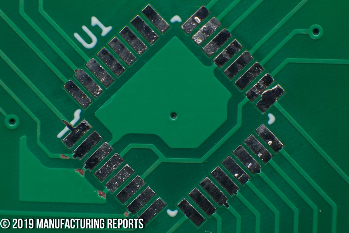
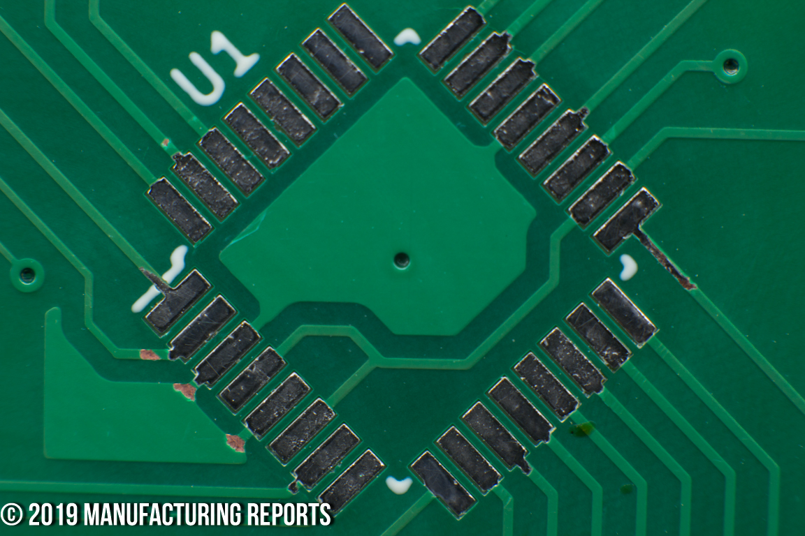
Solderability
A random board was selected and subjected to the solder and rework tests. It was difficult to get the QFP to sit flat on the pads, and some shoving around was necessary to finally get everything aligned correctly prior to drag soldering the sides of the chip that hadn’t been tacked down. However, after both the first and second round of rework, the solder mask showed excellent resiliency to the process. Slight erosion occured traveling away from the pads after the first rework, and some spots appeared in the ground pour outside the footprint. After the second round, the erosion over the traces continued to extend, but somehow the ground pour remained unaffected. In fact, the photo shows that after the second rework, no solder had adhered to what seemed like exposed copper.
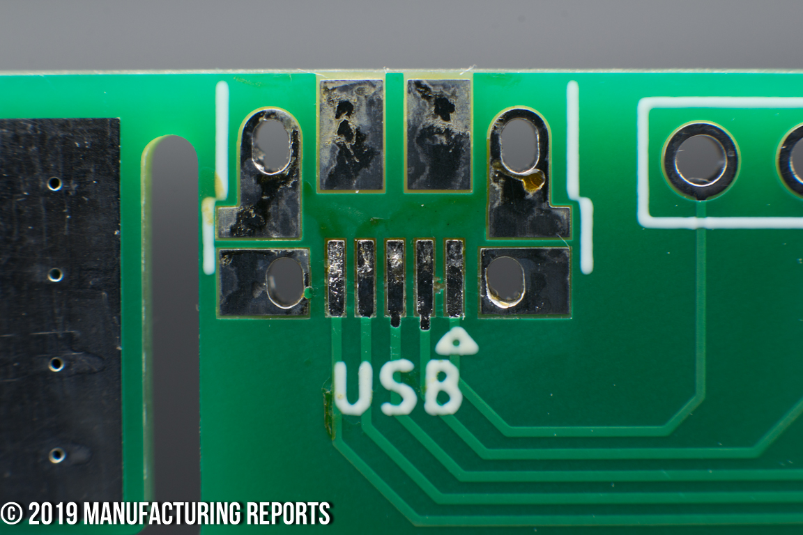
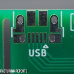
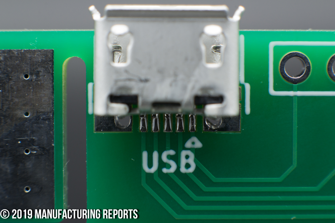
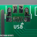
The Micro USB connector fared even better. It sat far more easily against it’s pads than the QFP, and after the first rework, showed negligible decay of the resist layer up the traces and none at all of the mask dam between the pads. The second rework eroded the web between the fourth and fifth pads but didn’t extend the decay over the traces by any measurable amount.
-
- QFP32 Before Soldering
-
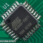
- QFP32 After Soldering
-
- QFP32 After First Rework
-
- QFP32 After Second Rework
-
- Micro USB Before Soldering
-
- Micro USB After Soldering
-
- Micro USB After First Rework
-
- Micro USB After Second Rework