ALLPCB PCB Service Review
ALLPCB
Guande, China
$0.90
1
3
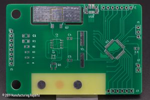
Manufacturing Reports Test Coupon v2
Excellent Ordering Options
Detailed Order Report
Customer Service Proactively Reached Out
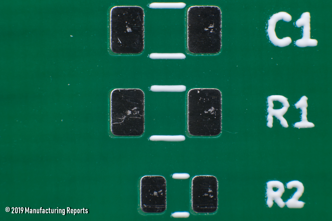
Very Crisp Silkscreen
Excellent HASL Surface Finish
Errors During Gerber Upload
Manufacturer's Mark Printed -- No Removal Option
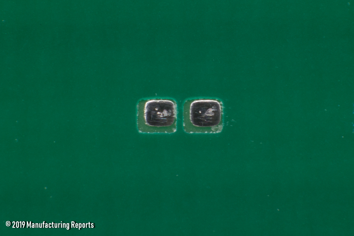
Horrible Solder Mask Keep Out
Very Thin Top Copper Layer
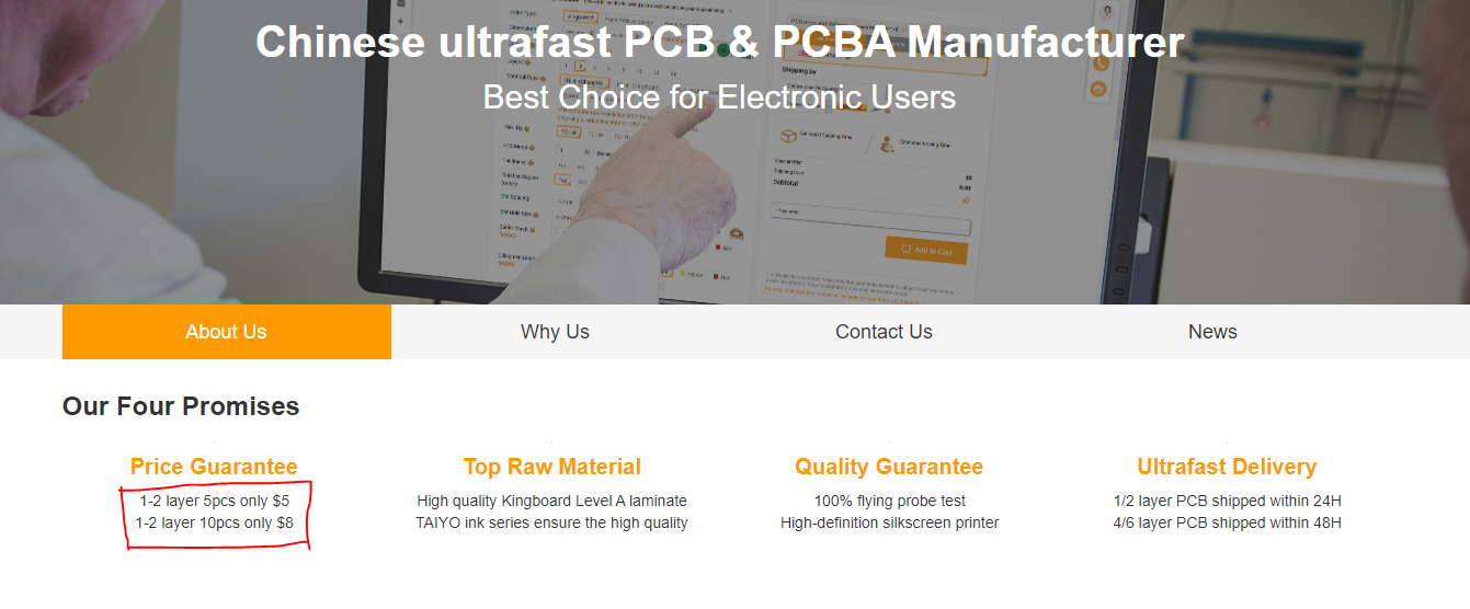
ALLPCB bills themselves right on their homepage as “World’s Fastest PCB Manufacturing”, and they express that the quality is “A-grade Military Material”. Their factory is located in Guangde, about 200km outside of Shanghai and no where near Shenzhen, which seems unique with so many other fabs and EMS just north of Hong Kong. ALLPCB claim to have independently developed their PCB quotation engine and the backend CRM system, while investing in top-of-the-line production and testing equipment, and hopefully this ALLPCB PCB Prototype Service Review will see if that makes a difference. Crucially, they publish four bold promises on their About Us page:
- Price Guarantee of “1-2 Layer 10pcs only $8”
- Top Raw Materials
- Quality Guarantee with 100% flying probe testing
- Ultrafast Delivery, with shipping in 24 hours.
Cost
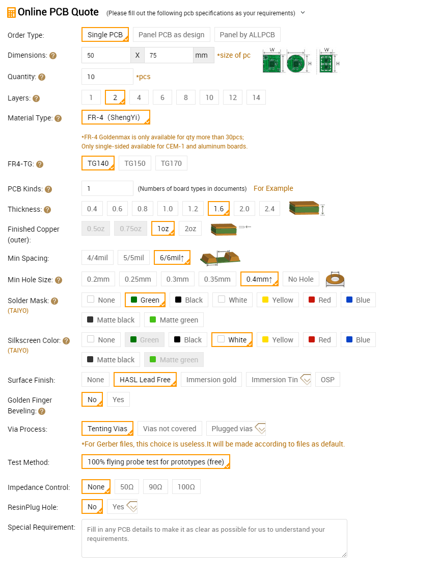
Right away ALLPCB violates their first promise of “Price Guarantee” by charging $9.00 for 10 copies of the test coupon. However, they charge around $5.00 less for expedited DHL shipping, at $17.00 rather than the usual $23.00 from factories in Shenzhen. Payment was processed with PayPal and a $1.09 Paypal Fee was immediately charged to bring the order total to $27.09. Throughout the ordering process, the checkout menu showed an expected shipping time of the next day, but after payment had been sent, the estimated shipping time was bumped back a day. Now, this may be my fault entirely for submitting an order on a Friday, GMT-7, but it still seems like a very, very minor bait-and-switch.
ALLPCB $8 Price Promise
A $5.00 instant discount is offered at checkout that I un-selected, and my guess is that it’s a “first time customer” offer.
Ordering
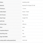
ALLPCBs “independently developed PCB quotation engine” looks remarkably like all the others that you find with offshore manufacturers. Unique to ALLPCB, orders of quantity 30 or more allow you to select different copper clad manufacturers: ShengYi, Kingboard or Goldenmax, however no explanation is offered for why you might want to select one over the other. At the 10 board quantity these reviews are based on, though, different FR-4 Tg levels are available with ShengYi as the sole laminate provider.
Lead Free HASL is the only option of HASL available as a surface finish, and it was nice to see OSP available as an option with no additional cost.
Immediately below the “Add to cart” button ALLPCB says that final payment is subject to an engineering review and that 5-10% of customers’ orders may need an extra charge. The fact that a board order might cost more after the fab has had a chance to evaluate it isn’t new, however a company pointing it out is refreshing. Unfortunately they also say right below that, “Manufacturing number will be added on your boards by default!” and I didn’t see an option to eliminate the marking.
Attempting to upload the gerbers in their 50kb zip file first resulted in a “file upload is too large” error, then on the second attempt an error popup written entirely in Chinese, and finally success on the third attempt (after reloading the page).
Paypal showed a string of Chinese characters as the payment recipient, however the order status page has a nice “proforma invoice” link that generates an HTML invoice useful for submitting expense reports.
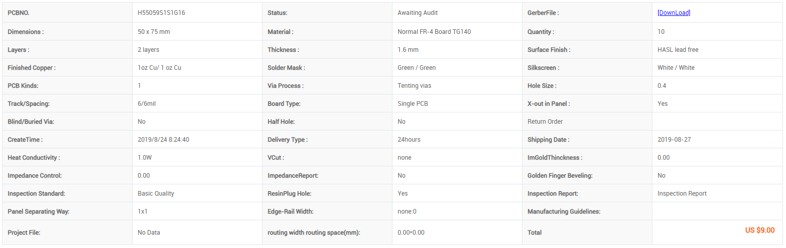
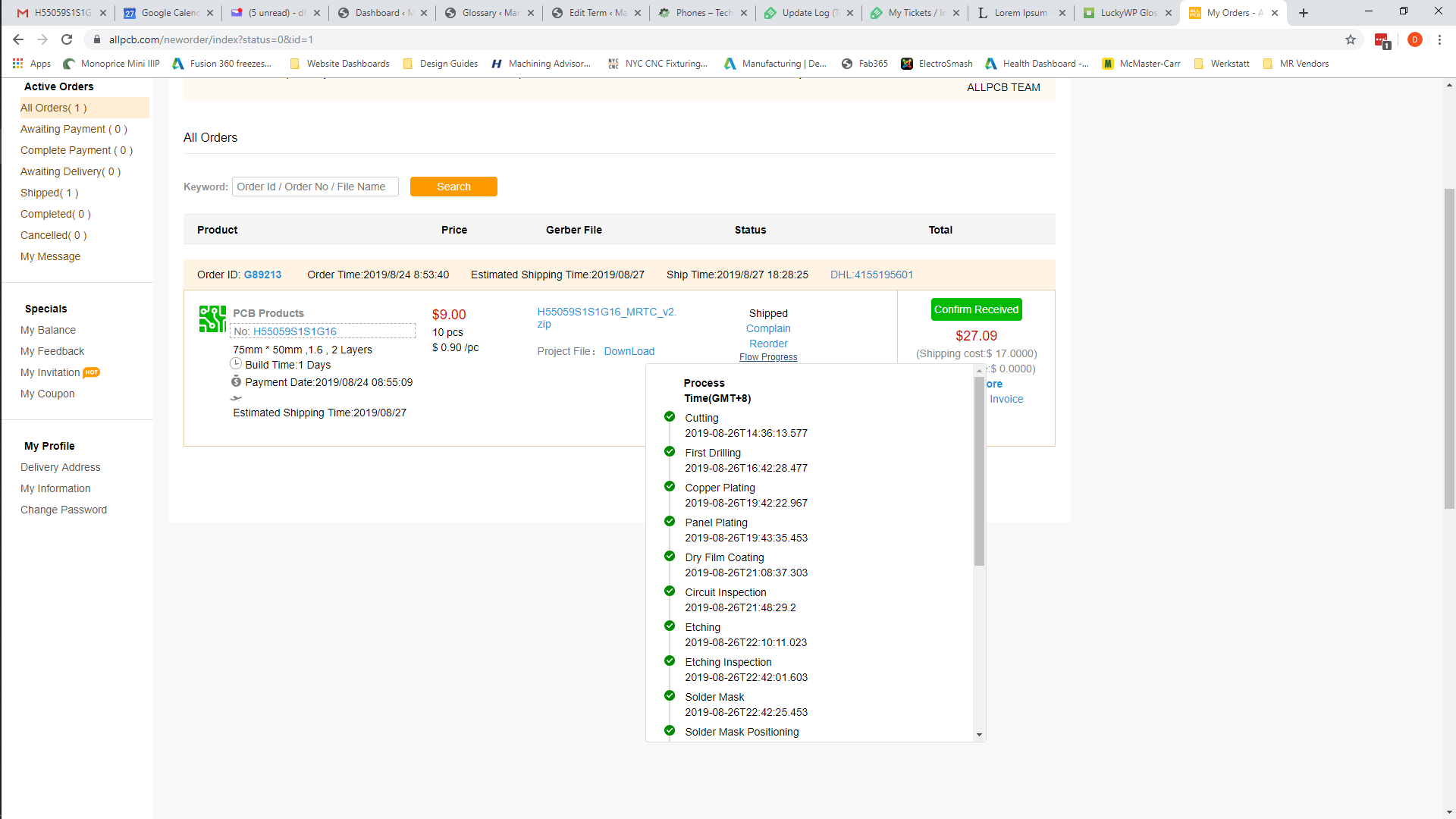
No gerber preview or board render is offered, however after submitting payment, you are given an extensive order report listing the stackup specification and order status.
-
- Order Options
-
- Order Report
Fulfillment
After three days had passed over the weekend, I received a shipping notification with a tracking number. The package was delivered in a standard DHL express pouch with a box inside. The boards were bundled together in a vacuum sealed bubble pouch which was placed loose inside the box. It rattled around a bit when I shook the box, but the boards didn’t appear any worse for wear when they were removed from the packaging.
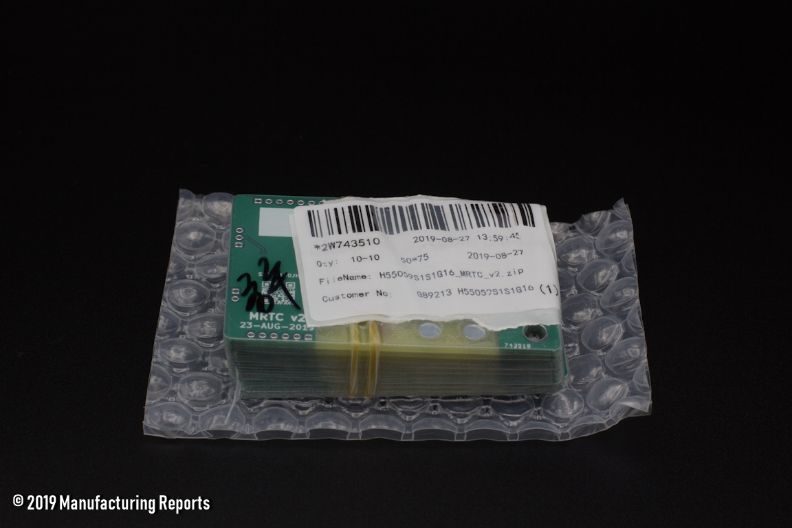
ALLPCB Board Packaging
Customer Service
Paypal inexplicably submitted an old shipping address, which happened when submitting payment for the PCBWay Service Review as well. An email was sent asking them to confirm the correct address and 20 minutes later ALLPCB responded with a copy of the invoice, asking me to confirm the ship to as listed.
On the order status page, ALLPCB has a very detailed order status, showing what they call “Flow Progress”. It time-stamps every fulfillment process from initial shaping to packaging and leaves no doubt as to what’s going on with one’s order. While the ordering interface didn’t seem very unique, this aspect of working with ALLPCB is probably reflective of the “independently developed CRM” claim.
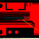
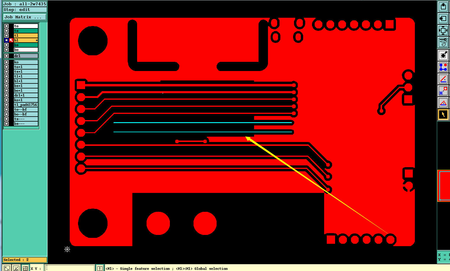
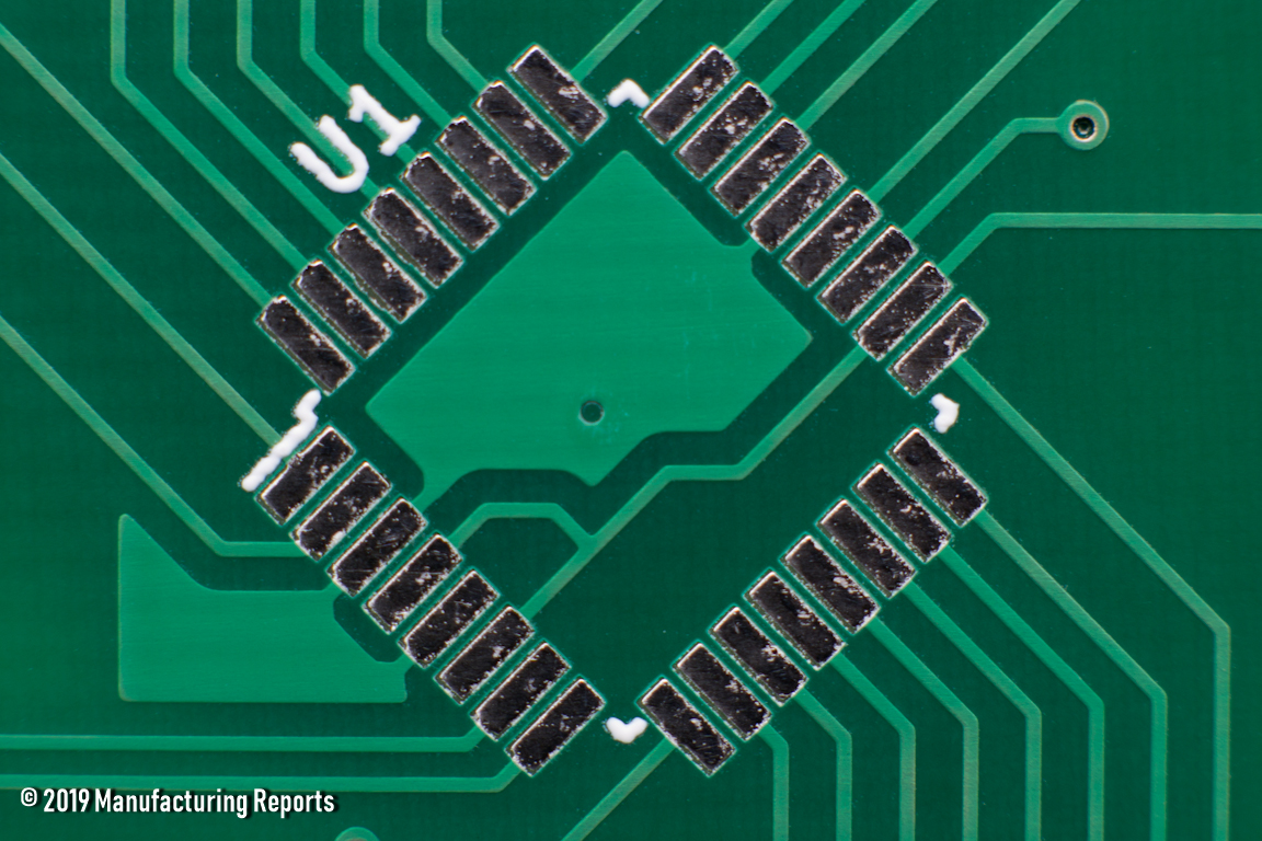
ALLPCB went a significant step further than other manufacturers in that they performed a design review and then, unprompted, sent me an email asking me to verify the need for certain features on the test coupon. Specifically they wanted to know if the 7 and 6 mil traces, which are unconnected to any nets, were necessary on the board, if the opening in the solder mask used to measure the trace widths was correct, and if the silk screen that would be printed directly onto the FR-4 could be moved onto the solder mask, or eliminated entirely. The questions were accompanied with images captured from their design review tool to make it clear which aspects of the design they were asking about.
There is a diligence there for a tiny order of 90 cent boards that feels above and beyond.
-
- Flow Progress
-
- Trace Width Design Review
-
- Silkscreen Design Review
-
- Solder Mask Design Review
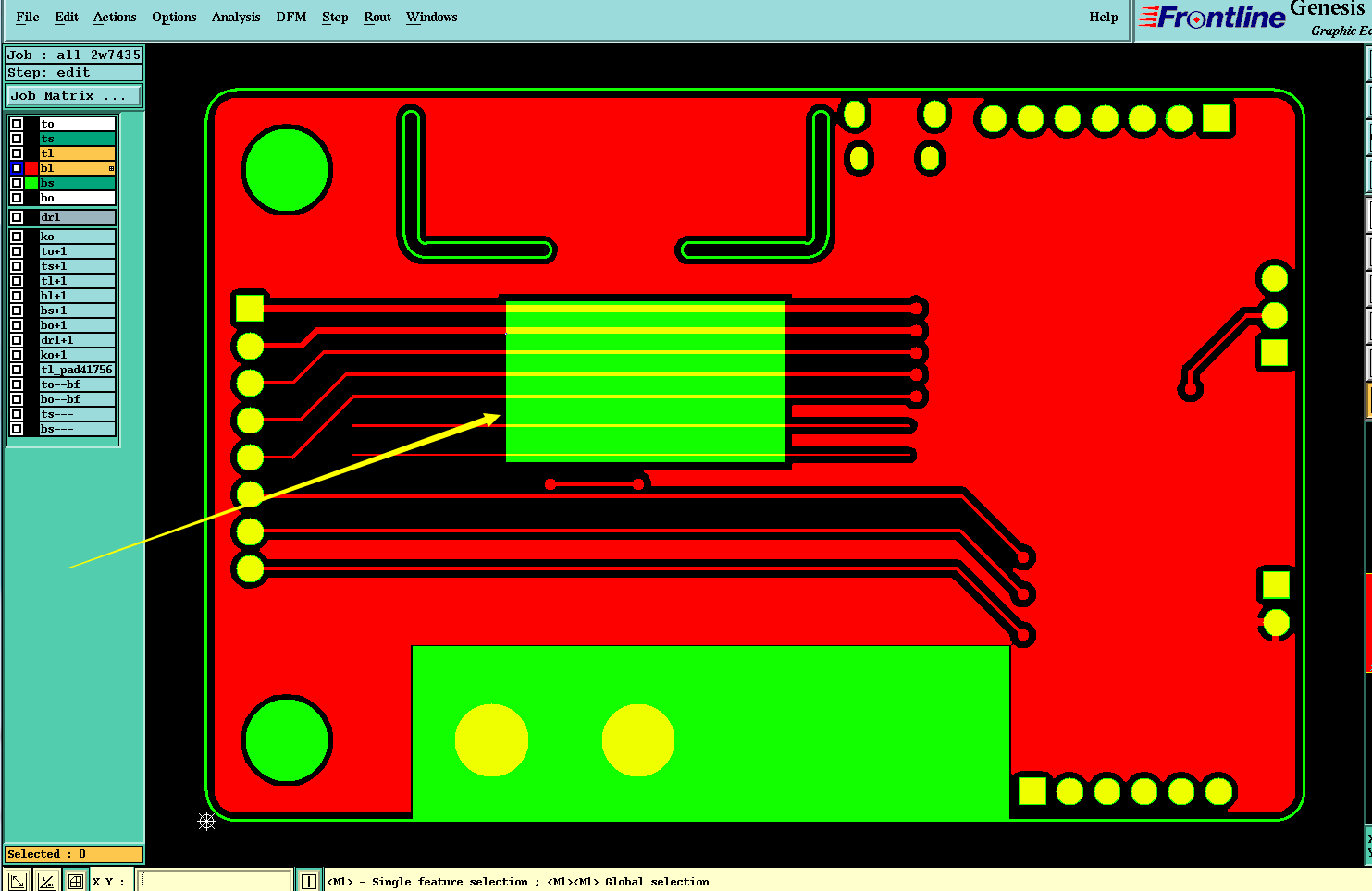
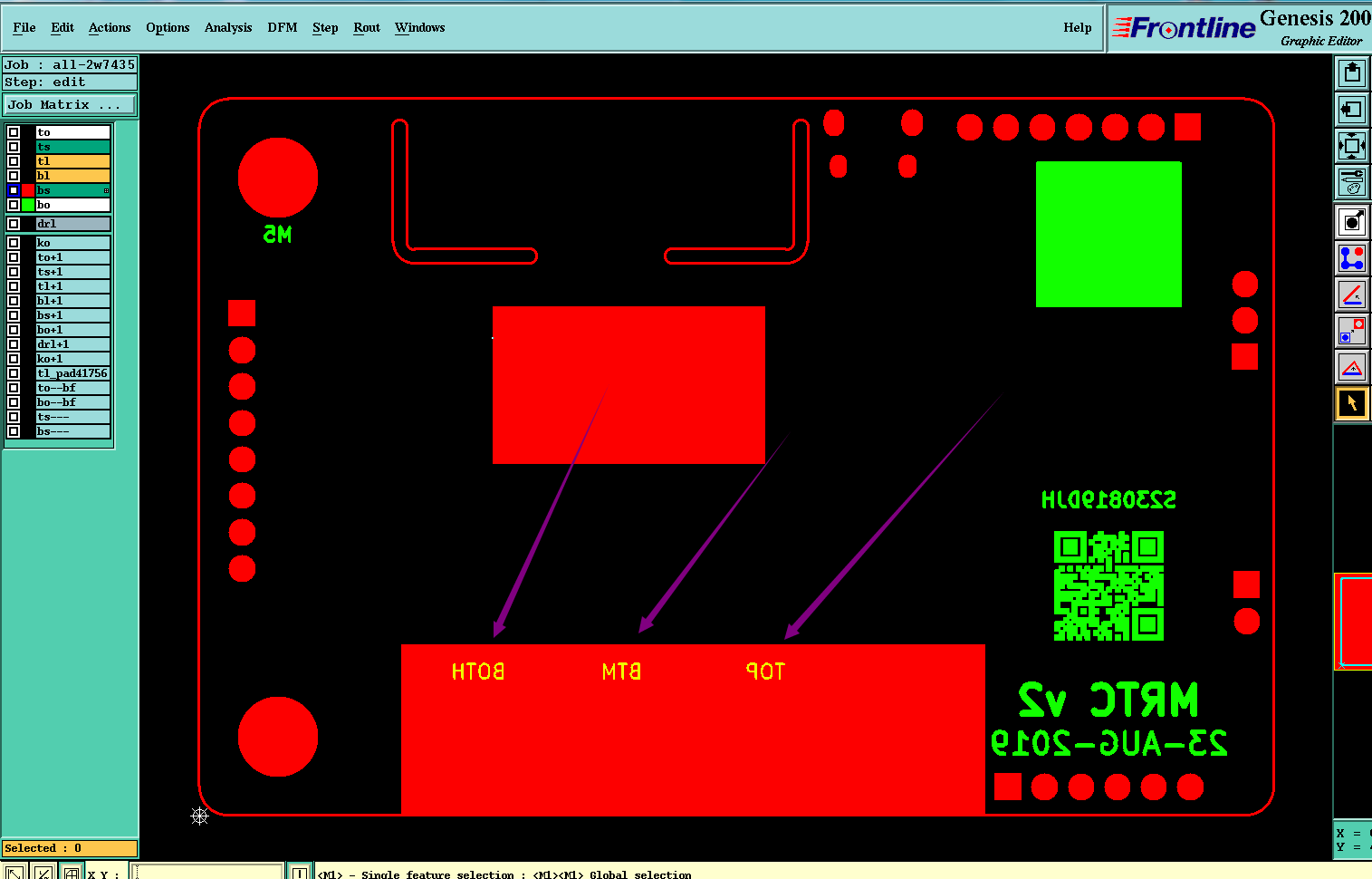
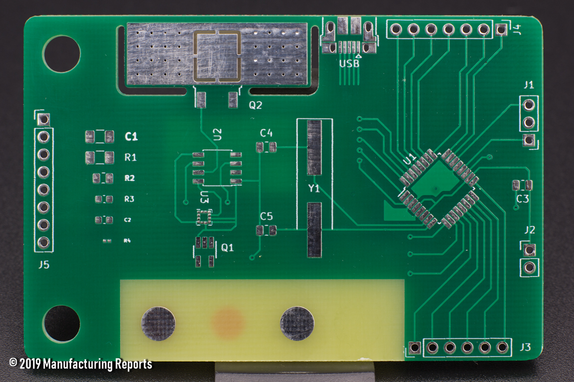
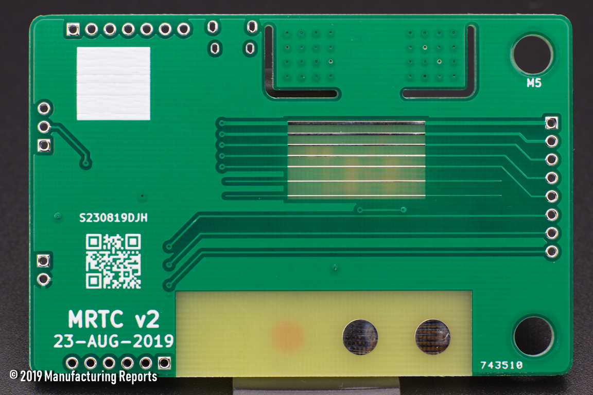
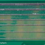
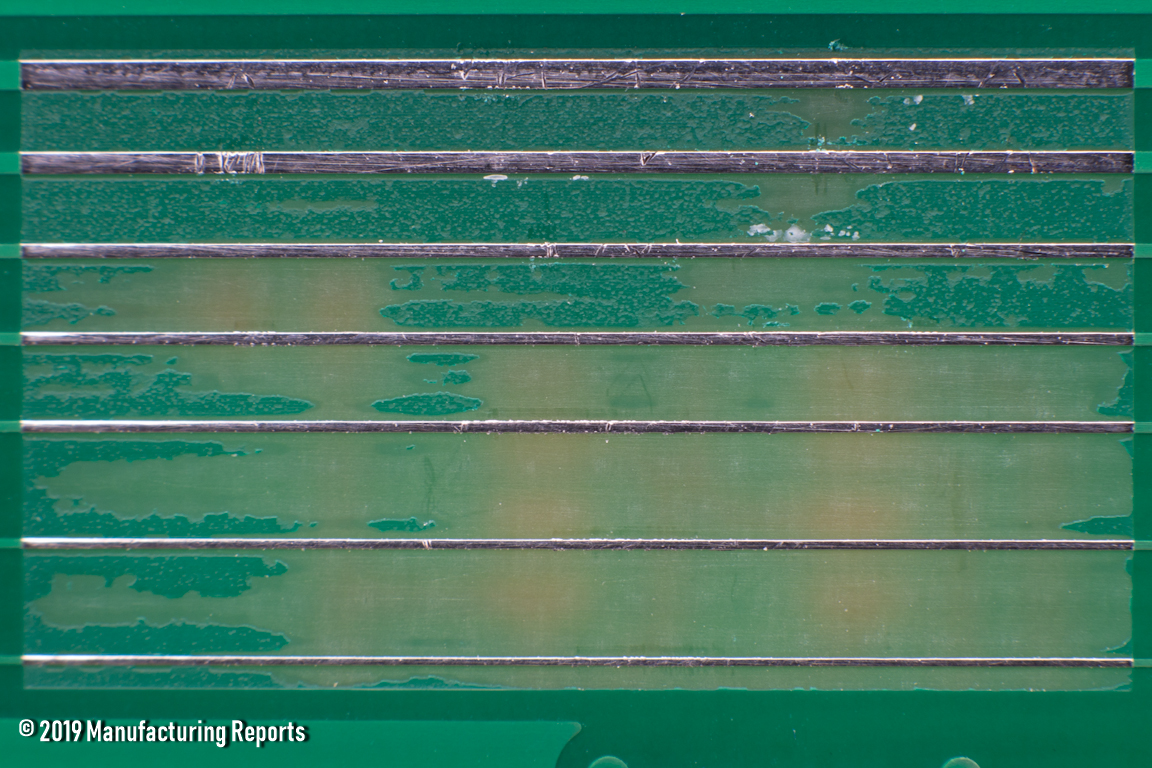
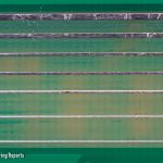
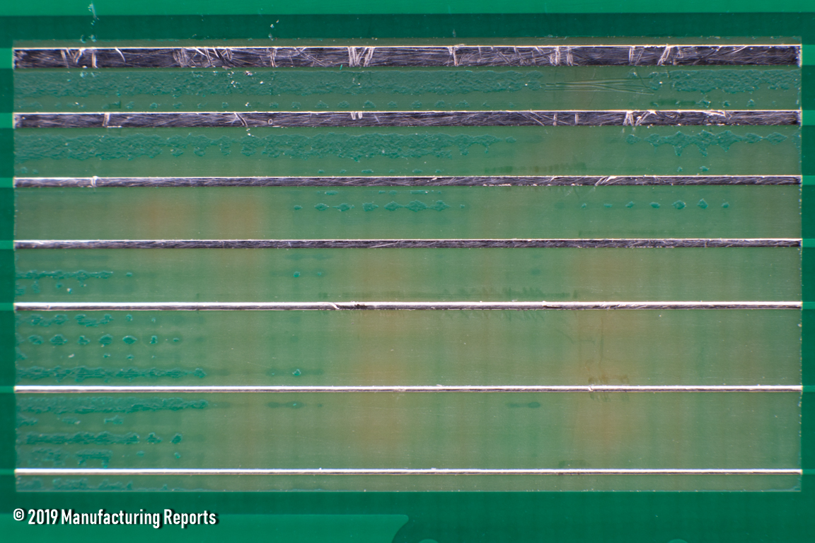
Circuit Board Visual Inspection
-
- ALLPCB Review Full Board Front
-
- ALLPCB Review Full Board Back
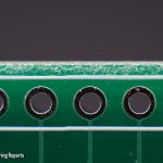
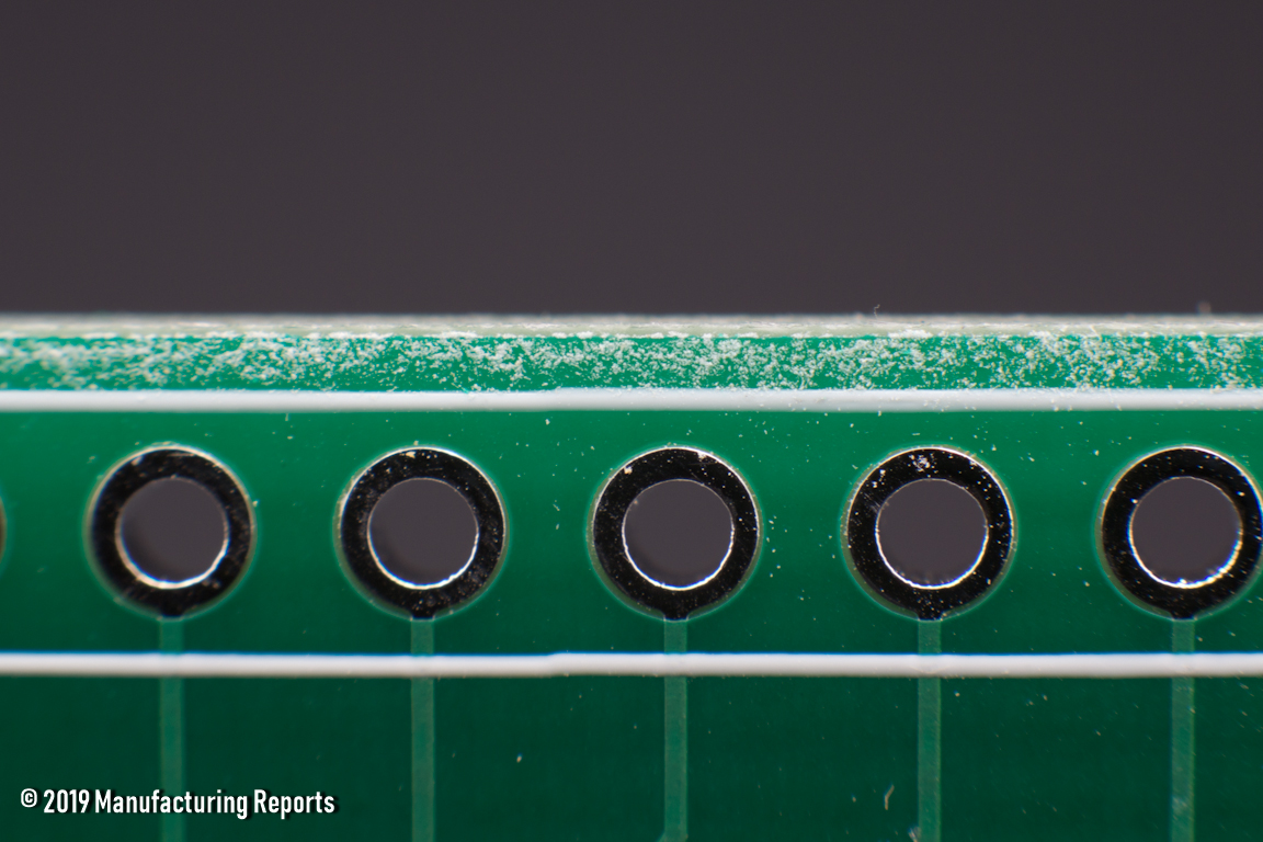
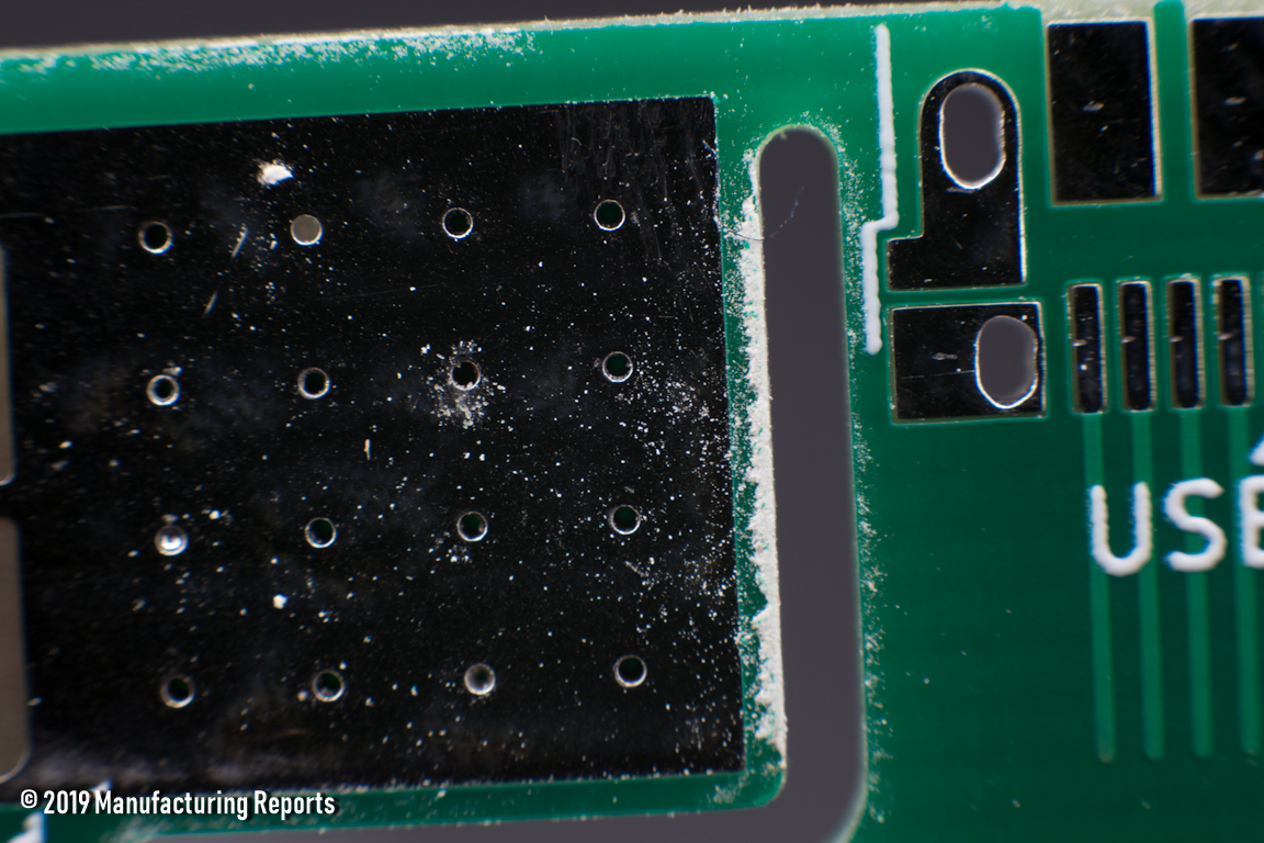
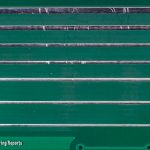
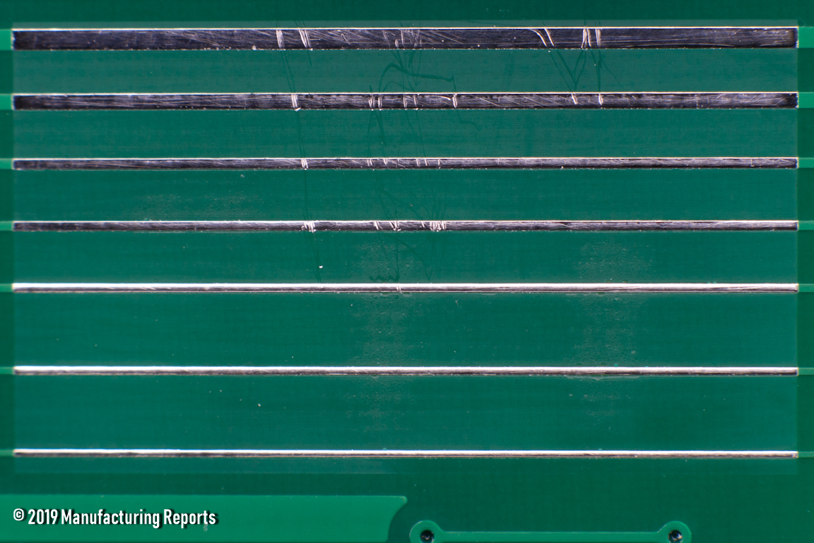
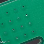
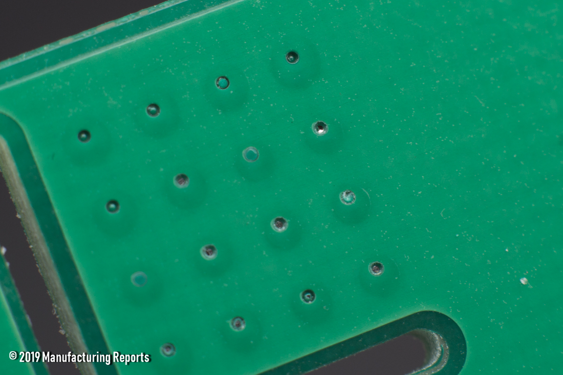
I complained about milling dust in the ShenZhen2U PCB Service Review, but I had to stop the visual inspection at least three times to take pictures of just how much FR-4 dust was coating these boards. At one point in the voice recording I took during the visual inspection, I remarked that I’d need to remember to wash my hands as soon as I was done so that I didn’t accidentally rub any particulate into my eyes.
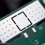
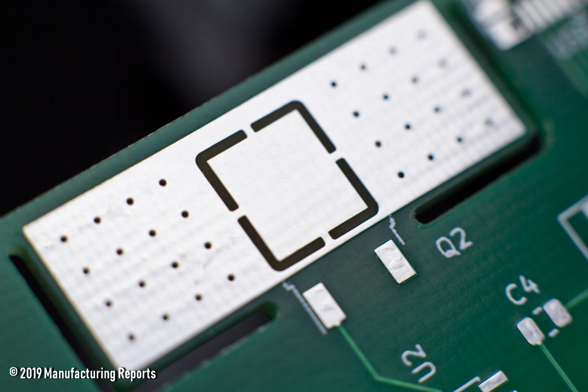
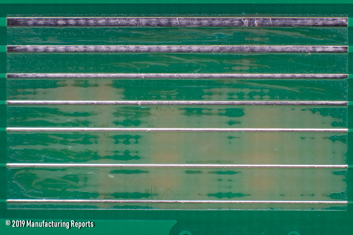
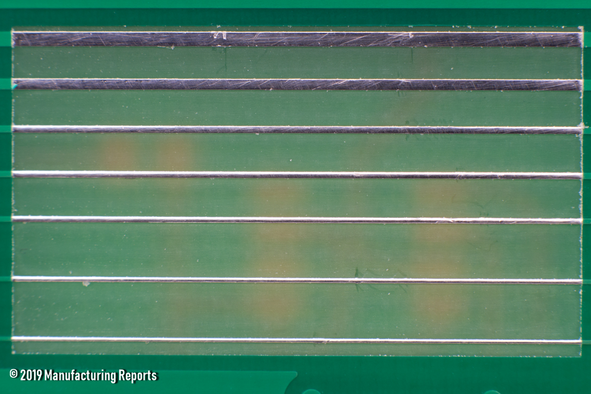
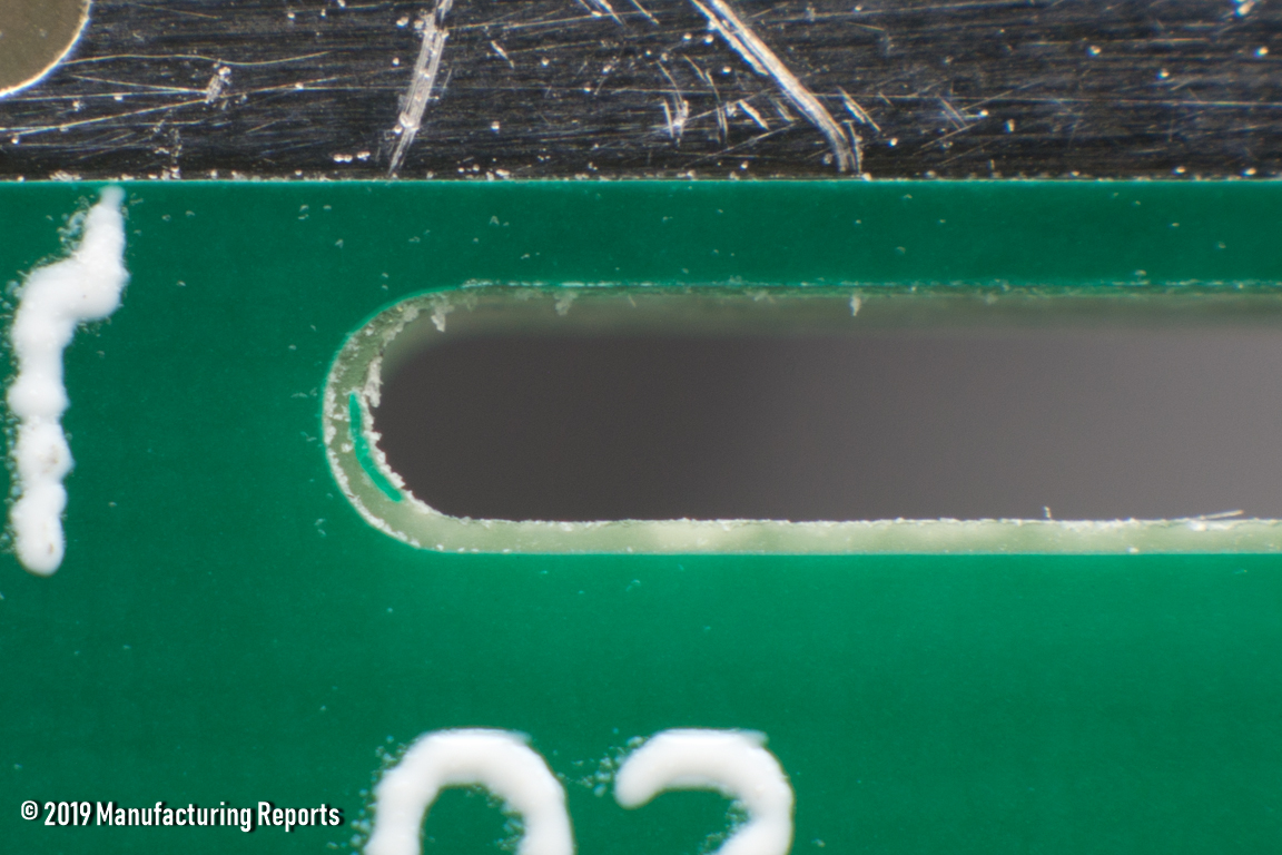
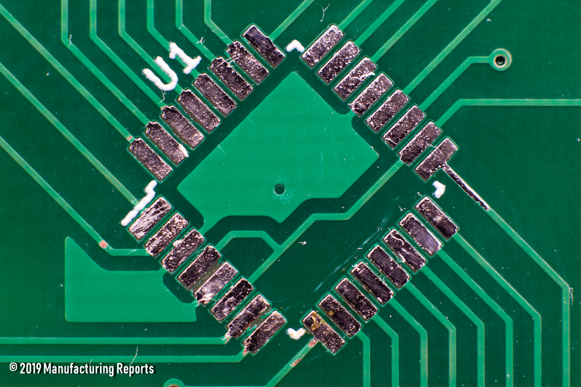
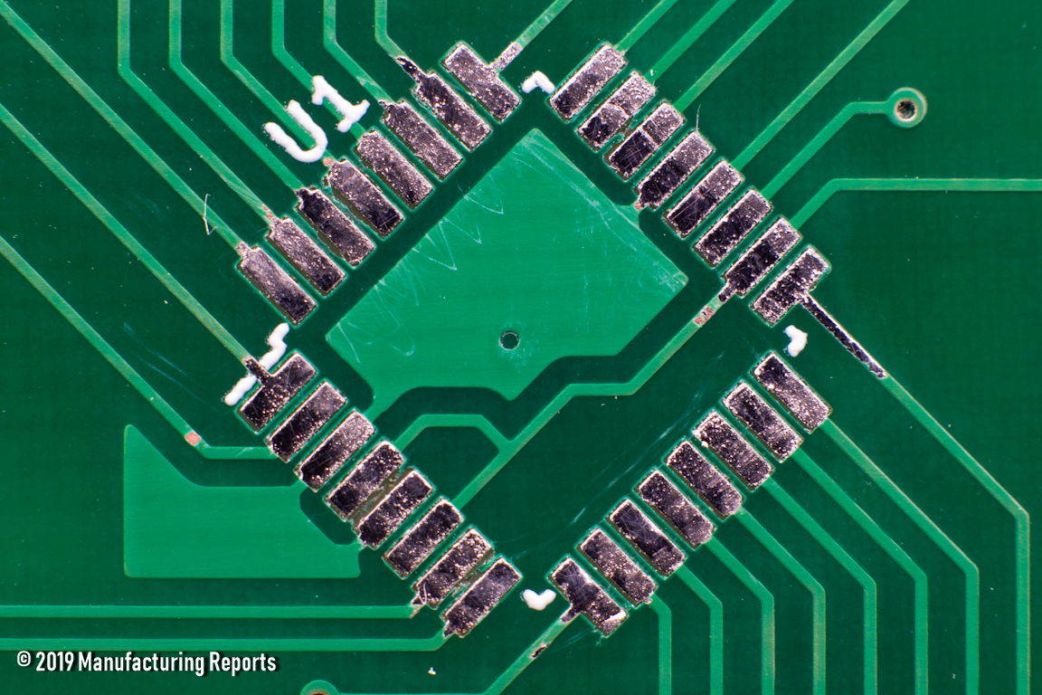
Unfortunately though, while the dust was an annoyance, the solder mask keepout was incredibly flawed. Six of the boards had solder mask residue in the trace width testing area, with one of those boards having a full skin of the mask material so thick that the traces couldn’t be measured — the calipers kept sliding off the top. As that was an area their customer service specifically called out as “are you sure you want us to do this”, I thought this would have been something guaranteed to be well executed.
In addition to the solder mask problems, the traces themselves failed the width tests in several instances, and the top copper was well below tolerance on all but two boards.
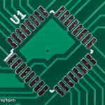
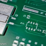
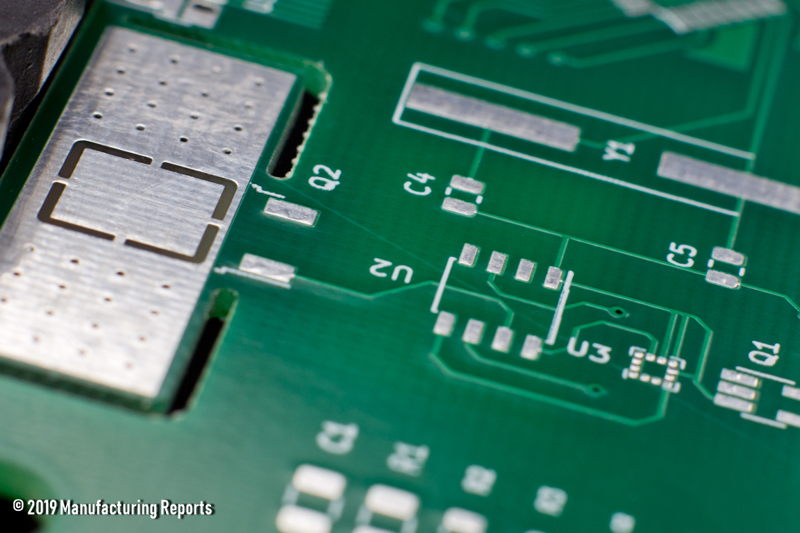
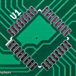
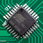
The HASL surface finish is very clean, and the silk screen is some of the best I’ve run across with these prototyping services. And while there were problems with trace width and copper thickness, the footprints are well fabricated from the QFP-32 down to the 0201 passive.
PCB Dimensions
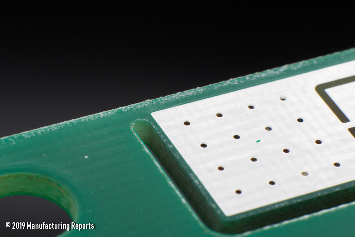
One of the first things I noticed was that many of the boards had very pronounced burrs on the edge cuts, detectable when just running the pad of your finger or dragging a fingernail along the edge of the PCB. That goes hand in hand with just how much dust was caked to these boards. In some cases I thought these were silk screen misprints until I wiped the board down and realized it was just clumps of FR-4 dust. Several of the boards had to be blown clean with compressed air because dust had packed into the vias.
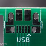
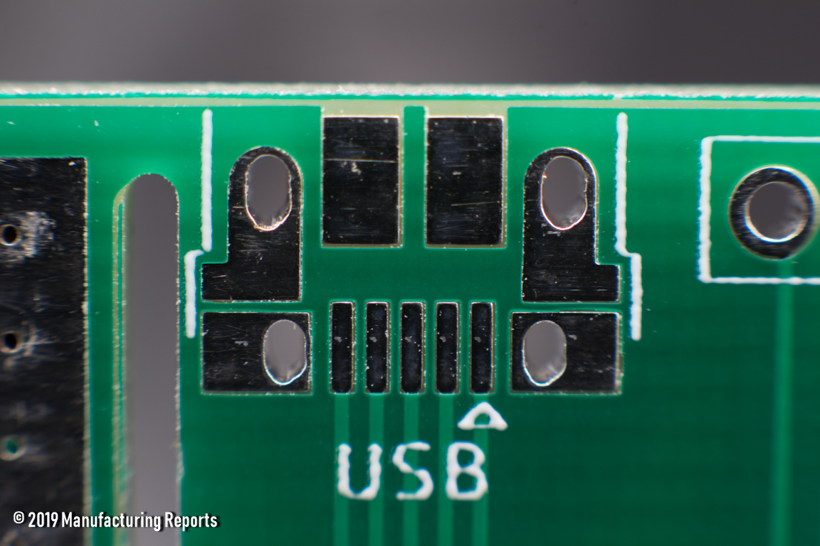
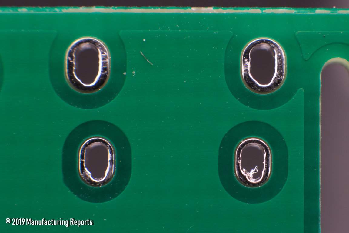
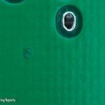
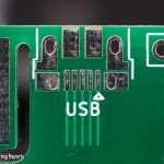
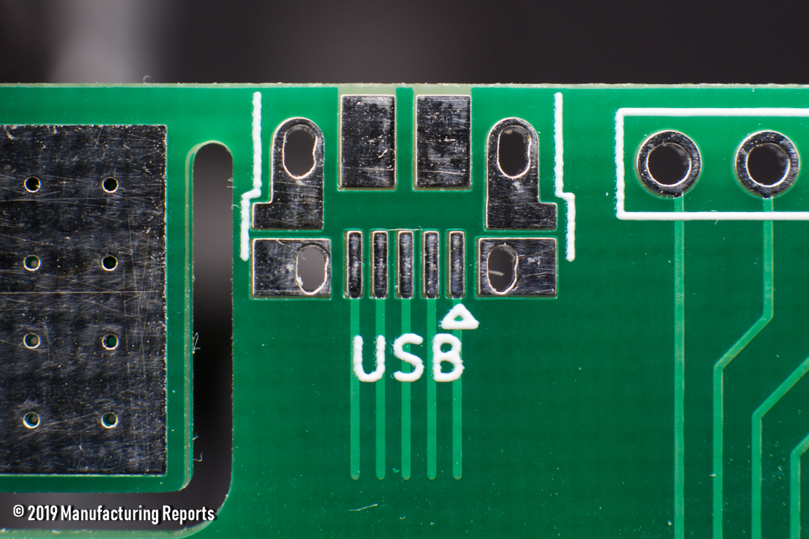
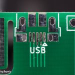
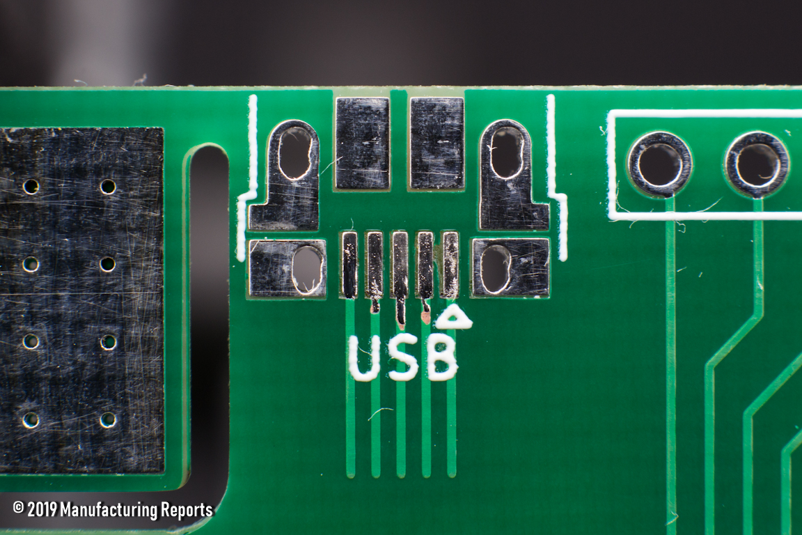
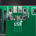
The dimensionality of the milled features, while covered in burrs, is very well executed, and above all consistent. Outer board edges were all well within tolerance, as were the mechanical holes and unplated slots. Positioning of the NPTH and PTH was spot on and fit the jigs well. The small plated slots at the USB connector were milled generally straight, but I would have preferred a little better consistency between boards. There’s nothing there that would prevent placement of that component though.
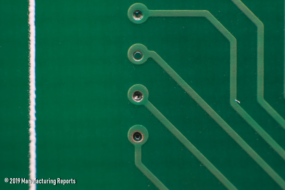
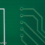
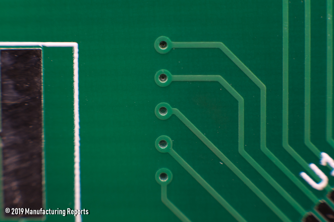
The via drills are spot on for the most part, with only a few here and there that seemed remarkably offset, and a couple boards where I even remarked out-loud how centered they looked.
Trace widths were a problem with almost all of them undersized across all boards, and in four cases measuring under tolerance. One board had so many problems with the solder mask that it prevented me from measuring the trace width.
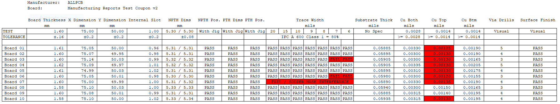
ALLPCB Test Report 2019
-
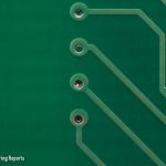
- Typical Via Drill Offset
-
- Beautiful Via Drills
-
- Nicely Milled Plated Slots
-
- Dust Clinging to Burr
-
- Dust On Edge Of Board
-
- Milling Dust Packed in Vias
-
- Dust and Frayed FR-4
-
- Absolutely Filthy Board
Copper Layer Quality
ALLPCB is the first company I’ve run across that publicly advertises the manufacturer of their copper laminate, in this case “Kingboard Level A”, although based on the ordering process I believe I received ShengYi laminate. Unfortunately, none of the websites associated with Kingboard Laminates or Kingboard Laminates Holdings Limited loaded at the time of publication so I couldn’t find out if that meant anything at all, and datasheets from ShengYi were equally as hard to come by..
There was a consistent mismatch in thickness between the top and bottom side copper layers so if that board was made with “Kingboard Level A”, Kingboard should do better quality control. 80% of the boards failed the thickness tolerance test for the top layer of copper.
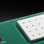
I really liked the HASL finish on these boards. It is uniformly flat and free of gaps and embedded impurities. It is well applied over the heatsink area, and only in a few spots appears to have wicked through to the back of the PCB.
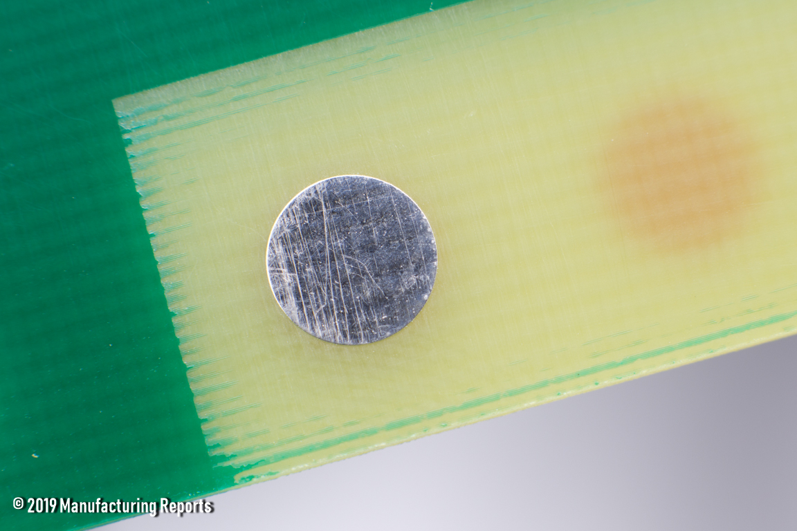
The traces aren’t damaged anywhere I could find, although they are undersized across all the boards, dramatically so in a few instances. The few noticeable scratches that run across the surface of two of the PCBs don’t seem to have penetrated the solder mask, as testing showed no conductivity between the scratched area and the ends of the traces.
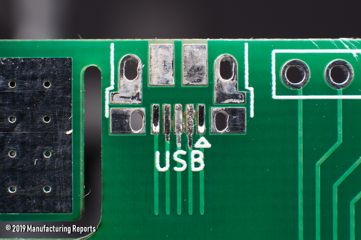
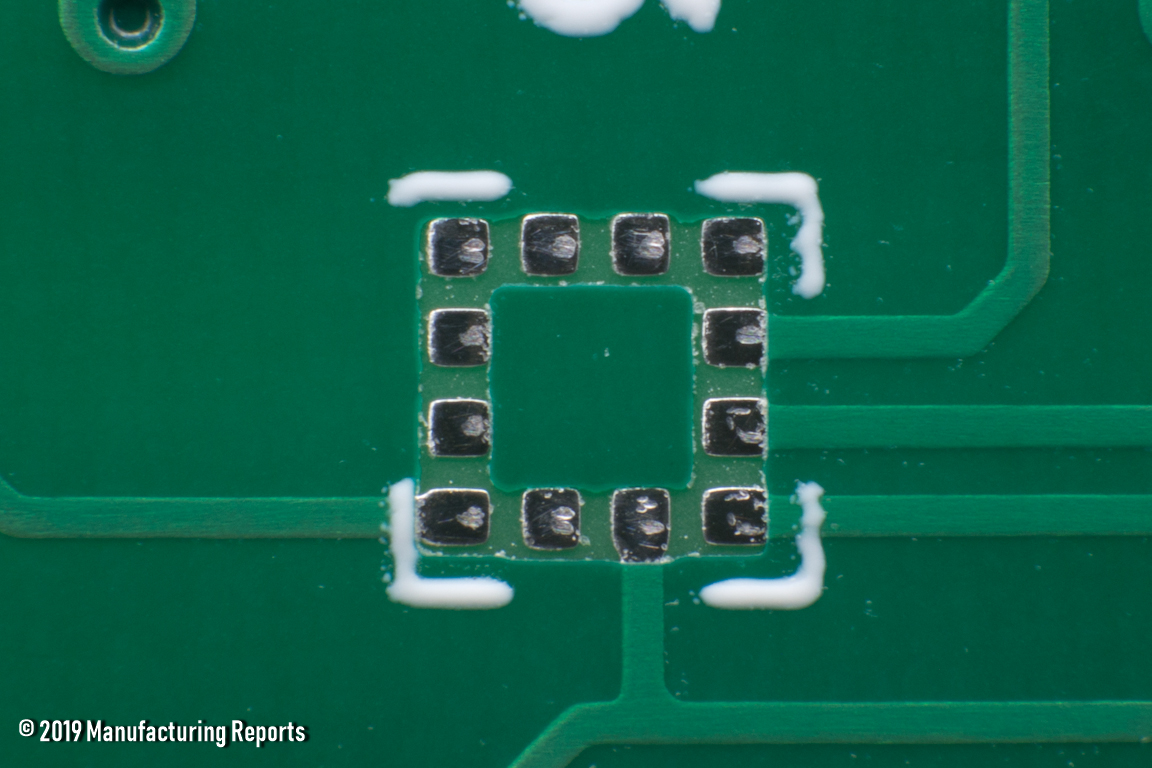
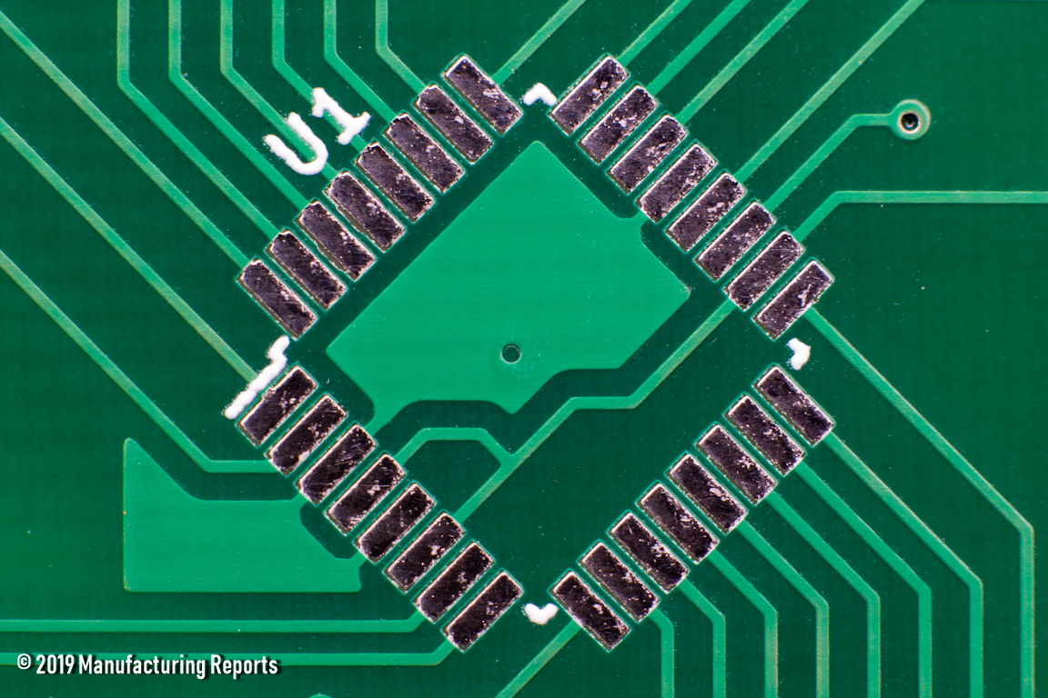
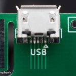
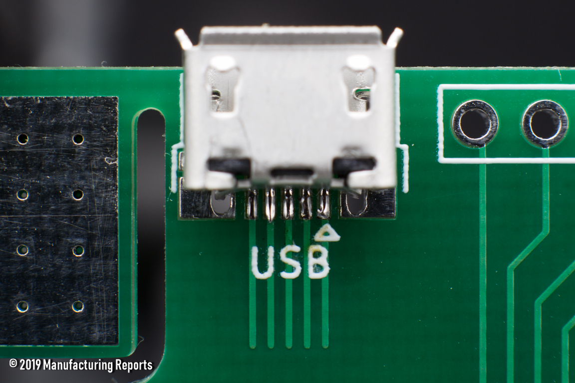
The QFP and QFN footprints are consistently well manufactured, as are the passives footprints from the 1206 all the way down to the 0201. The USB Connector was also well formed across all boards, with one little errant spike of HASL surface finish clogging one footprint.
-
- QFP Footprint
-
- QFN Footprint
-
- 1206 Footprints
-
- 0201 Footprint
-
- HASL Finish over Heat Sink
-
- Surface Scratch by XTAL
-
- Surface Scratch Through SOIC8
-
- HASL Clog in USB Footprint
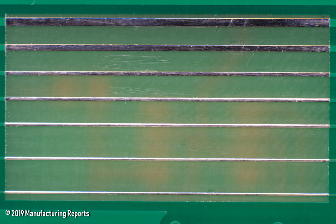
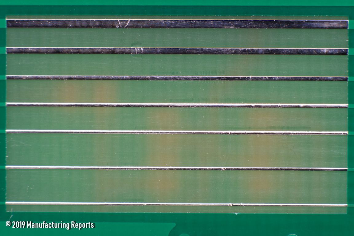
Solder Mask Quality
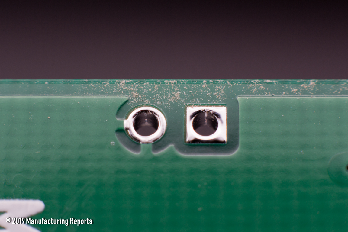
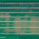
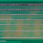
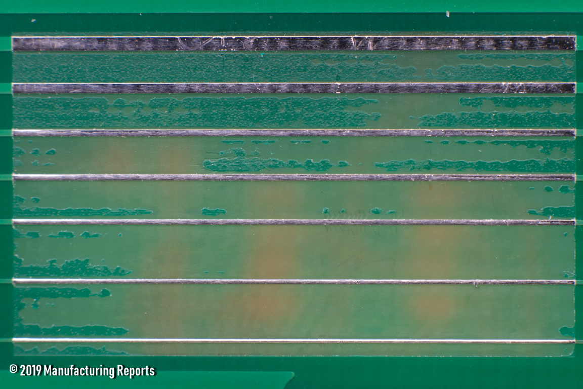
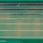
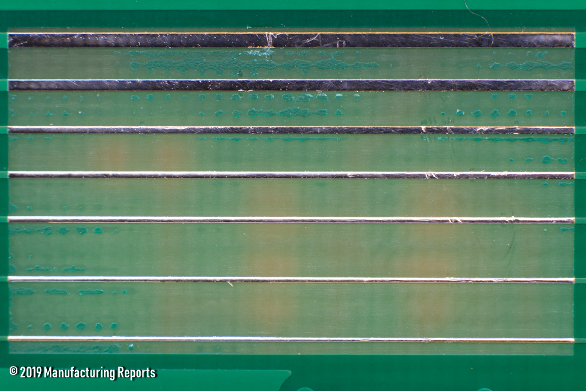
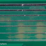
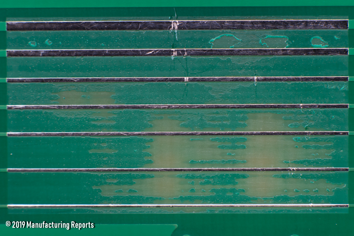
I simply don’t understand how a manufacturer would let boards that look like this ship to the customer. At best, the mask residue left behind on some of the boards is equivalent to trying to pull a really bad paper sticker off of a new product only to have the adhesive stay 80% put and keeping half of the paper with it. At worst, there was such a thick film of resist layer left, that I found it impossible to measure the width of the traces in that area.
I’m astonished because you don’t need magnification or microscopes or macro lenses or bright lights to see this. It’s obvious — all someone had to do was care enough to look. So either they never looked and shipped it, or they looked and figured “we’ll care if they complain”, and shipped it.
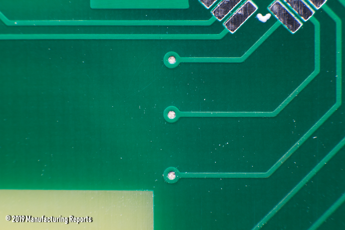
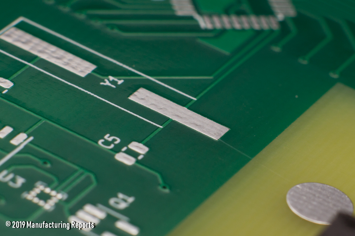
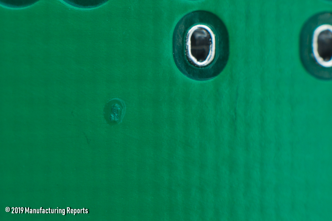
Beyond those issues, on some boards the mask layer appears visibly thin, exposing the annular ring around the via drill. As mentioned above, there is also a visible scratch across two of the boards, but tests indicate that it’s not through to the copper underneath. There are a few minor issues with contaminant either under or embedded in the solder mask as well.
Which is a shame, because thin solder mask, non-critical scratches and a couple of contaminants away from pads are not perfect, but they’re not disqualifying. Screwing up by not ensuring the resist layer is gone from the area I specifically called out, and that you double checked in the design file, is disqualifying.
-
- Solder Mask Board 01
-
- Solder Mask Board 02
-
- Solder Mask Board 03
-
- Solder Mask Board 04
-
- Solder Mask Board 05
-
- Solder Mask Board 06
-
- Solder Mask Board 07
-
- Solder Mask Board 08
-
- Solder Mask Board 09
-
- Solder Mask Board 10
-
- Front Solder Mask Issue
-
- Large Offset With Rough Milling
-
- Clean Mask Over Stitching – Minor Wicking
-
- Contaminant Under Mask
Silkscreen Quality
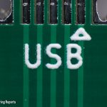
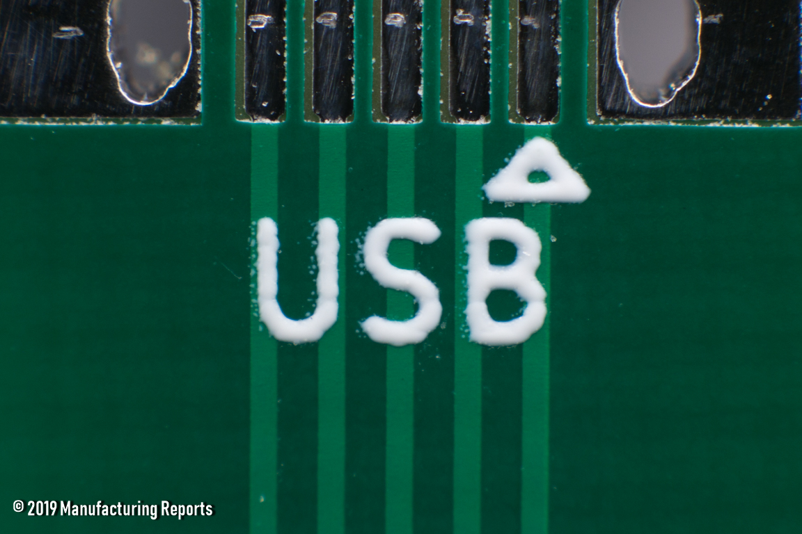
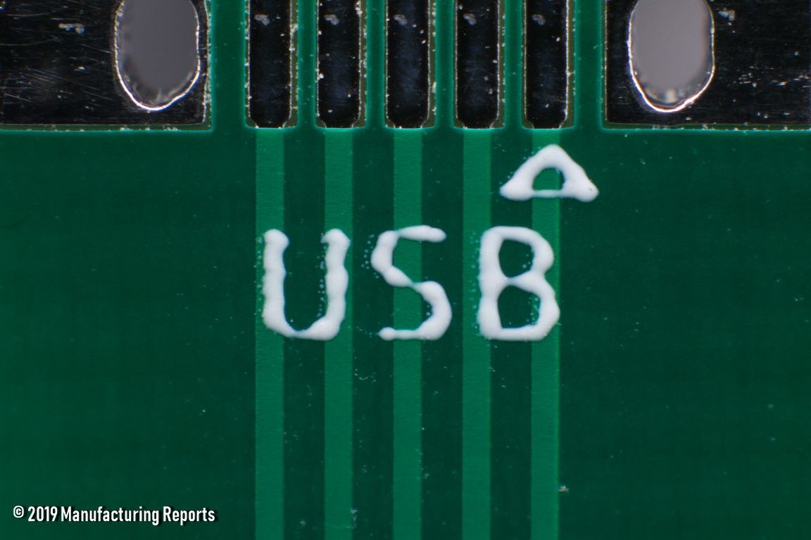
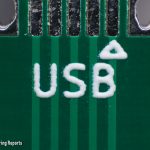
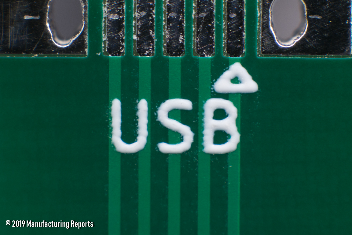
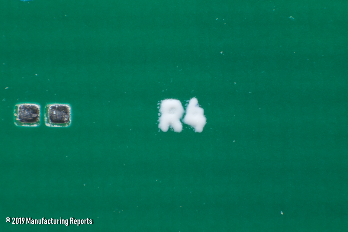
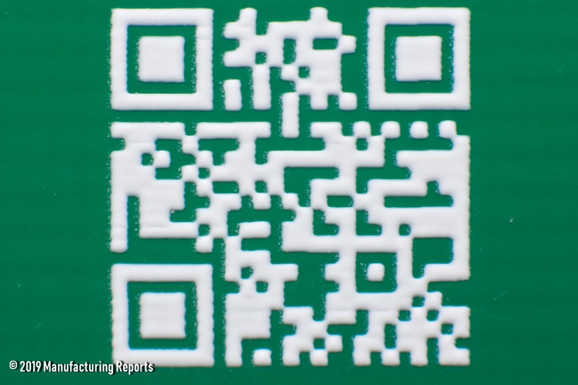
The silkscreen from ALLPCB is well executed with few inconsistencies. The printing is applied using a DLP process, so occasional blotchiness and puffiness of the artwork and fonts is expected. On the back silk layer, the QR Code was very well reproduced, allowing code scanning directly with no magnification at all. The text printed over varying z heights was the area of inconsistency, but only on a few boards and then only in a few areas.
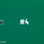
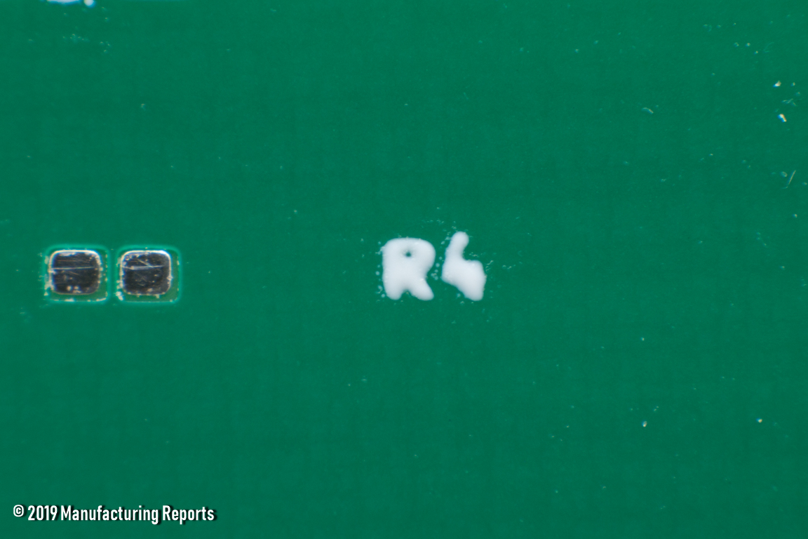
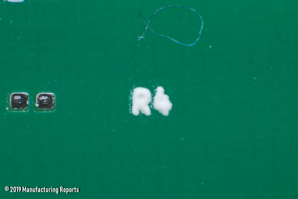
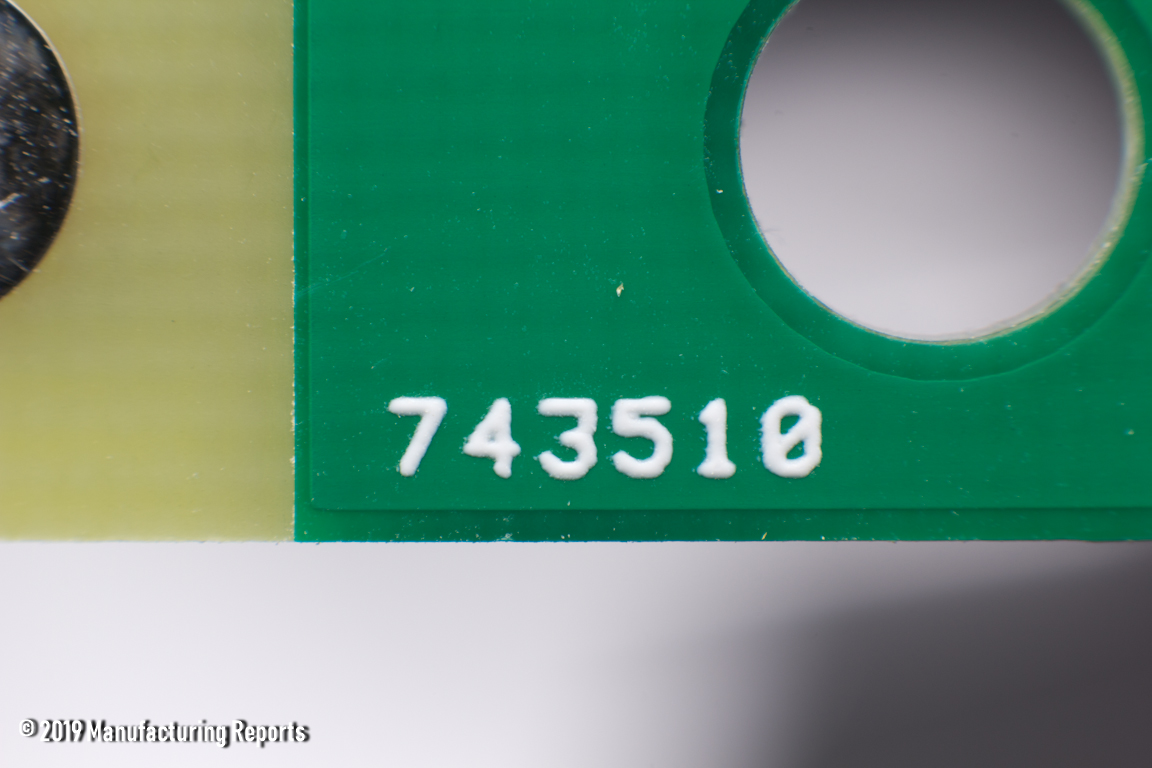
There were no overprints, misprints or cosmetic blemishes found, however a manufacturer’s mark was applied on each bottom silk layer by the lower M5 clearance hole, and there was no option to have that removed during ordering.
-
- Silk over Varying Z Height Ex. 01
-
- Silk over Varying Z Height Ex. 02
-
- Silk over Varying Z Height Ex. 03
-
- Small Font Reproduction Ex. 01
-
- Small Font Reproduction Ex. 02
-
- Small Font Reproduction Ex. 03
-
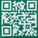
- QR Code
-
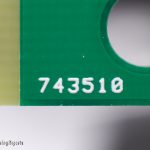
- Manufacturer’s Mark
Solderability
The ALLPCB board stood up well to the two rounds of rework, although after the second round, the micro USB solder mask had really begun to erode between the pads. Both the microcontroller and the USB connector sat flat on their pads and were easy to solder down.
The first round of rework showed some spots of solder mask missing along the traces leading to the QFP, with the largest path of erosion extending 2mm from the pad on the far right. Looking at the micro USB after rework, I saw the mask layer beginning to break down between the pads, and erosion creeping up the traces as well.
The second rework didn’t seem to cause as much degradation of the resist as the first round, increasing around 0.5mm from a few pads. The micro USB suffered more, as the mask completely disappeared between several pads, exposing the substrate underneath.
-
- QFP Before Soldering
-
- QFP After Soldering
-
- QFP After First Rework
-
- QFP After Second Rework
-
- Micro USB Before Soldering
-
- Micro USB After Soldering
-
- Micro USB After First Rework
-
- Micro USB After Second Rework